Flat Silicon Substrates for Research
A PhD candidate contacted UniversityWafer requesting affordable silicon wafers
to use as flat substrates for laboratory research.
Researcher Inquiry
“I am interested in purchasing silicon wafers for a relatively basic
substrate application. I need affordable
4-inch silicon wafers
with
(100) crystal orientation
and a high-quality
single-side polished surface
.
I do not want reclaimed wafers, but I am unfamiliar with the available
silicon wafer grades
.
I have previously used Prime grade wafers and would like to understand
whether
Test grade silicon wafers
or another lower-cost grade would be suitable.
I would prefer low dopant concentrations and higher resistivity, but I do
not require premium high-purity silicon. Please let me know which in-stock
wafers best match these specifications.”
This type of application may be suitable for Prime, Test, or research-grade
wafers depending on the required flatness, surface finish, resistivity, and
defect tolerance.
Reference #99494 for related specifications and historical
inquiry details.
Request Substrate Specifications and Pricing
Tell us the substrate material, diameter, thickness, orientation, surface
finish, resistivity, coating, and quantity required for your research.
UniversityWafer can help identify suitable in-stock or custom substrate options.
Get Your Substrate Quote FAST!
Or,
Buy Online
and start researching today!
Indium Nitride Layers on Sapphire Substrates
A chemical engineering professor contacted UniversityWafer regarding
indium nitride wafers, InN powder, and the possibility of depositing an
InN layer on a suitable crystalline substrate.
Researcher Inquiry
“Do you have indium nitride wafers or InN layers deposited on a substrate?
We may also be able to use particulate InN if sufficiently high-purity
material is available.”
Potential InN Material Options
Depending on the research requirements,
polycrystalline InN
may be available in powder form. Thin InN coatings may also be investigated
using deposition methods such as electron-beam evaporation, sputtering, or
epitaxial growth.
A
sapphire substrate
may be considered for InN deposition because sapphire is widely used as a
base substrate for III-nitride materials. However, lattice mismatch, thermal
expansion, film stress, cracking, and defect density must be evaluated before
selecting a deposition process.
MOCVD Growth on Sapphire
Metal-organic chemical vapor deposition (MOCVD)
is commonly used to grow III-nitride materials such as
GaN on sapphire
.
Similar growth concepts may be investigated for InN, although the achievable
thickness and crystalline quality can be limited by material stability and
lattice mismatch.
InN, GaN, AlN, and sapphire have different lattice parameters. These
differences can produce strain, dislocations, defects, and cracking as the
deposited layer becomes thicker. Buffer layers and carefully controlled
growth conditions may therefore be required.
Substrates for III-Nitride Research
Custom InN deposition should be evaluated as a research project rather than
assumed to be a standard stocked product. Feasibility, target thickness,
substrate choice, deposition method, characterization requirements, and
project cost should be confirmed before work begins.
Reference RFQ #109936 for the original research inquiry and
related specifications.
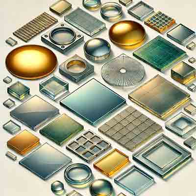
What Is a Substrate?
A substrate is the base surface or material on which another material,
coating, device, or structure is deposited, grown, or fabricated. The meaning of
substrate varies by field, but in semiconductor manufacturing and materials science,
it commonly refers to a wafer, glass plate, crystal, or other solid surface used to
support a fabrication process.
-
Biology: A substrate may be the surface or medium on which cells,
microorganisms, or other organisms grow.
-
Chemistry: A substrate may refer to the substance involved in a
chemical or enzymatic reaction.
-
Electronics: A substrate is the base material on which circuits,
sensors, transistors, and semiconductor devices are fabricated.
-
Materials Science
:
A substrate supports thin films, coatings, nanomaterials, crystals, and other
deposited structures.
In semiconductor research, the most widely used substrate is the
silicon wafer
.
Depending on the application, researchers may also use
silicon-on-insulator (SOI) wafers
,
sapphire substrates
,
silicon carbide (SiC)
,
gallium arsenide (GaAs)
,
or
gallium nitride on sapphire
.
Substrates for Thin-Film Deposition
Substrate selection is especially important in
thin-film deposition
,
where surface roughness, flatness, thermal stability, chemical compatibility,
crystal orientation, and electrical properties can affect film adhesion and
device performance.
Common substrate materials for
chemical vapor deposition (CVD)
,
epitaxy, surface chemistry, sputtering, evaporation, and related coating processes
include silicon, glass, quartz, sapphire, metals, and compound semiconductors.
Silicon Wafers
Silicon
is the most common substrate material used in semiconductor fabrication,
microelectronics, MEMS, surface chemistry, and thin-film research.
Silicon wafers provide a smooth, stable, and highly controllable surface for
depositing films and fabricating electronic devices.
-
Common diameters:
100 mm,
150 mm,
200 mm, and
300 mm.
-
Crystal orientation:
Common
silicon orientations
include (100), (110), and (111).
-
Doping:
Wafers may be supplied as
P-type silicon
,
N-type silicon
,
or high-resistivity silicon.
-
Surface finish:
Single-side polished, double-side polished, unpolished, or prepared for
epitaxial growth
.
-
Flatness:
Low
total thickness variation (TTV)
is important for lithography, bonding, deposition, and device fabrication.
Researchers may also select
epitaxial silicon wafers
,
thermal oxide wafers
,
or
silicon nitride wafers
when the application requires a specific surface layer, dielectric coating,
or device structure.
Glass Substrates
Glass substrates
are widely used for optical coatings, sensors, microfluidics, displays,
microscopy, wafer bonding, and dielectric research. Available options include
borosilicate glass, fused silica, display glass, and conductive glass.
-
Borosilicate glass
for chemical, microfluidic, and wafer-bonding applications.
-
Fused silica
for optical, high-temperature, and thin-film applications.
-
BK7 glass
for optical components, windows, and coatings.
-
Borofloat 33
for MEMS, microfluidics, and anodic bonding.
-
D263 glass
for thin, flexible, and optical substrate applications.
-
ITO-coated glass
for transparent electrodes, displays, sensors, and optoelectronic devices.
Metal and Coated Substrates
Metal-coated substrates are commonly used in catalysis, electrochemistry,
plasmonics, biosensors, electrical contacts, and surface science.
Researchers may use
gold-coated silicon wafers
when high conductivity, chemical stability, or a noble-metal surface is required.
Substrates Used in Electronics
In electronics, substrates provide the mechanical and electrical foundation
for microchips, integrated circuits, transistors, photodetectors, power devices,
sensors, and other components.
Monocrystalline Silicon
Monocrystalline silicon
is the primary substrate used for semiconductor devices because of its high purity,
controlled electrical properties, mature processing technology, and compatibility
with
photolithography
.
-
(100) silicon:
Commonly used for integrated circuits, MOS devices, and general semiconductor fabrication.
-
(111) silicon:
Frequently selected for anisotropic etching, MEMS, epitaxy, and specialized research.
-
Polished silicon:
Provides the smooth surface required for high-resolution processing and deposition.
-
Epitaxial silicon:
Adds a controlled crystalline layer for advanced electronic devices.
Silicon-on-Insulator Substrates
Silicon-on-insulator wafers
contain a thin device layer separated from the silicon handle wafer by a buried
oxide layer. SOI substrates are used for MEMS, photonics, RF electronics,
low-power devices, and advanced transistor research.
Alternative Semiconductor Substrates
Applications involving high power, high frequency, high temperature,
optoelectronics, or infrared detection may require semiconductor materials
other than silicon.
-
Sapphire (Al2O3)
:
Used for LEDs, RF devices, optical components, epitaxial growth, and
harsh-environment applications.
-
Silicon carbide (SiC)
:
Used for high-power, high-voltage, high-frequency, and high-temperature electronics.
-
Gallium arsenide (GaAs)
:
Used for RF electronics, optoelectronics, lasers, solar cells, and
high-speed semiconductor devices.
-
Gallium nitride on sapphire
:
Used for LEDs, power electronics, high-frequency devices, and
wide-bandgap semiconductor research.
-
Germanium (Ge)
:
Used for infrared optics, photodetectors, solar cells, and semiconductor research.
Specialty and MEMS Substrates
Glass, silicon, SOI, quartz, and sapphire substrates are also used in
microelectromechanical systems. Researchers developing sensors, actuators,
resonators, and microfluidic devices can learn more about
substrates for MEMS fabrication
.
Substrates Used in Materials Science
In materials science, substrates are selected according to the intended
deposition method, operating temperature, lattice compatibility, optical
transparency, electrical conductivity, surface finish, and chemical resistance.
Silicon for Materials Research
Silicon wafers are frequently used for thin-film growth, nanostructure fabrication,
microscopy, coating evaluation, surface modification, and electrical testing.
Researchers can select wafer diameter, thickness, orientation, resistivity,
doping type, and surface finish to match the experiment.
Sapphire Substrates
Single-crystal sapphire substrates
provide high hardness, optical transparency, thermal stability, and electrical
insulation. Sapphire is particularly important for the epitaxial growth of
gallium nitride and other optoelectronic materials.
- C-plane (0001): Commonly used for GaN epitaxy and LED research.
- A-plane: Used when nonpolar growth or alternative crystal alignment is needed.
- R-plane: Selected for specialized optical and epitaxial applications.
Quartz and Fused Silica Substrates
Fused silica substrates
offer high optical transparency, low thermal expansion, electrical insulation,
and resistance to elevated temperatures. They are commonly used for optical
coatings, thin-film deposition, microscopy, photonics, and high-temperature processing.
Applications requiring crystalline piezoelectric or frequency-control materials
may instead use
single-crystal quartz wafers
.
Conductive and Transparent Substrates
Transparent conductive substrates such as
indium tin oxide (ITO)
combine optical transparency with electrical conductivity. These substrates
are commonly used for displays, electrodes, solar cells, biosensors,
electrochemistry, and optoelectronic research.
How to Select a Research Substrate
The best substrate depends on the requirements of the fabrication process
and the intended device. Important selection factors include:
- Substrate material and crystal structure
- Diameter, shape, and thickness
- Single-side or double-side polishing
- Surface roughness and total thickness variation
- Crystal orientation and off-axis angle
- Electrical resistivity and doping type
- Optical transmission range
- Thermal expansion and processing temperature
- Compatibility with deposition, etching, or wafer bonding
UniversityWafer supplies semiconductor, optical, glass, crystalline,
dielectric, and coated substrates in standard and custom specifications
for university, laboratory, prototype, and production applications.
Explore Related Substrate Materials
