Thin Film Coated Wafers for Research and Production

university wafer substrates

Vacuum Deposition Experts

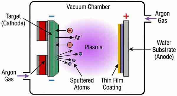
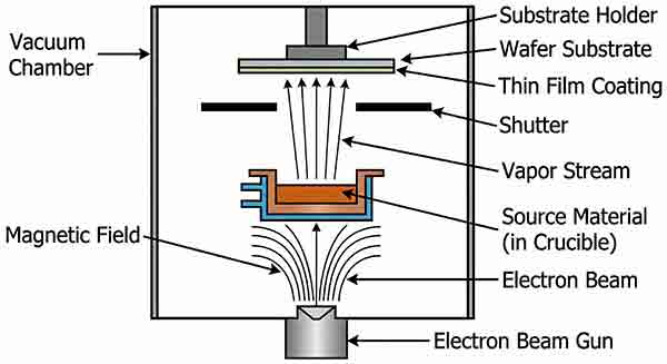
UniversityWafer, Inc. and our partners provide custom sputtering and e-gun evaporation services:

We Provide R&D and Production

We help researchers in all there research, development and production needs in both academia and industry. Below are just some industries that we cater to.

  • Biomedical, biotechnology
  • Ultrasound
  • DNA sequencing
  • Medical devices and implants
  • Diagnostics and therapeutics
  • MEMS, instrumentation, sensors, microelectronics, displays
  • Energy storage and conversion
  • Solar, optical
  • Aerospace
  • Government labs, universities

Get Your Thin Film Quote FAST!

Substrates We Can Supply or You Can Supply!

  • Customer-furnished substrates that we have coated:
  • Silicon
  • Compound semiconductors
  • Glass, including fused silica, borosilicate, and soda-lime
    Ceramics, including alumina and aluminum nitride
  • Sapphire
  • Plastics and polymers, including foils
  • Metal foils and plates
  • PZT
  • Wafers patterned with lift-off photoresist
  • Wafers with cantilevers and deep-etched topographies

How to Deposit Carbon on Silicon?

A research client asked us the following:  

I am looking for wafers coated with a carbon thin film. I am interested in both amorphous or glassy carbon about 1-2 microns thick. Do you know if anything like that exists?

I was thinking of a 4" Si wafer. Ideally the carbon layer would be be on SOI with the oxide and Si ~2microns thick. The carbon on 2-3 microns SiO2 would be good too. The carbon should be low stress. I am guessing I would need to purchase the SOI wafer and then grow my own carbon, but I wanted to see if by chance something similar like that already exists.

UniversityWafer replied:

Our historically maximum sputtered C thickness is 3,080Å.
If we push our sputtering process, we anticipate a maximum thickness of 8,000Å.

We do not know if it is amorphous or glassy.

We do know that n = 1.25 and k = 0.50 @ 632.8nm. This means that our sputtered C is a mixture of diamond and graphite.

Researcher:

Thank you for your response, this is interesting information. What is the reason for the upper limit? The nature of carbon films seems very variant, DLC, glassy, amorphous....mixture of Sp3/sp2.... I am interested in an electrically conducting film, best not shiny, so a mixture of diamond and graphite is ok, not too much diamond, which is typically not a problem! How much would 4" SOI wafer cost with the carbon sputtered on them? I cn chose the SOI wafer from your list, but could you let me know what the additional cost of the carbon would be and wha the minimum wafer count is? Also, do you know what the surface stresses are?

UniversityWafer, Inc.

Thank you for your response, this is interesting information. What is the reason for the upper limit? In this case the upper limit is set by a full day (8 hours) of deposition time. We are unable to run any deposition longer than 8 hours.

The nature of carbon films seems very variant, DLC, glassy, amorphous....mixture of Sp3/sp2.... Yes, we do not have a characterized C film, except for the n and k values reported earlier.

I am interested in an electrically conducting film, best not shiny, so a mixture of diamond and graphite is ok, not too much diamond, which is typically not a problem! The film is weakly conducting. The sheet resistance is high, outside of the range of our 4-point probe.

How much would 4" SOI wafer cost with the carbon sputtered on them? I cn chose the SOI wafer from your list, but could you let me know what the additional cost of the carbon would be and wha the minimum wafer count is? Our lot charge for in-situ sputter etch followed by sputter deposition of 8,000Å C is $3,300. Lot size = up to 12 wafers, 100mm dia. This job is considered as Experimental Work, to be done on a best efforts basis. Please refer to paragraph 8 in the attached Terms and Conditions of Sale.

Also, do you know what the surface stresses are? We have no data on film stress at this time. But we hope to have some data within the next few days.

New data as of today: Stress of sputtered C film (100nm thick): 913 MPa (compressive).

Introduction to Thin Film

What is a thin film educational video.


What Are Thin Films Used For?

Thin films are layers of material, ranging in thickness from fractions of a nanometer to several chemically deposited nanocrystalline metal oxide thin films by fabian i ezema chandrakant d lokhande rajan jose editorsmicrometers. The process of deposition involves depositing materials in controlled ways. For example, household mirrors are made of a thin metal coating on the back side of glass. This metal layer is reflective, making it useful in many applications. Silvering was the traditional method for producing mirrors, but now, the process is known as sputtering.

Today, thin films are used in many areas. They play a crucial role in materials research, and are often used to study quantum phenomena. The most common method for depositing thin films is through thin-film deposition, where layers are built up to a desired thickness. Different methods use different processes, including chemical vapor deposition, atomic layer deposition, molecular layer deposition, and electroplating.

These films are used in the semiconductor industry. They improve the transmittance and touch features of touch panels, and protect electronic devices. They also improve the lifespan of displays and other electronic components. This makes them vital to the advancement of technology. But, what are they used for? Let us find out! What Are Thin Films Used For? Once You Know About Them, You'll Wonder: "What Are They Good For?"

In addition to enhancing the visual appeal of many materials, thin films can enhance the performance of electronics and semiconductor devices. The films can alter the surface color, glossiness, or texture. And the applications for thin films are truly limitless. The following are some of the most popular. You can start by exploring your own creative ideas and experimentation to find out which ones work best for your needs. And remember: if it works for you, it's likely that it will work for you.

As you can see, thin films are essential to human life. The first application of a thin film for optical purposes dates back to 1912. This method of producing mirrors involved vaporizing metals in high vacuum. They were used to improve the quality of lenses, thereby improving their clarity and durability. The process of evaporating metals was first used to make lenses in the early twentieth century. The use of the film in the field of optics has since evolved dramatically.

Thin films are essential for a variety of technological applications. In the semiconductor industry, they are used to protect optical elements on lenses and protect displays from scratching. They can also be used to improve the durability of display panels. This is why thin films are so important in these industries. You'll find them everywhere. So, if you want to enhance the features of your device, you must know what thin films are.

There are many uses for thin films in the semiconductor industry. Some examples include telecommunication devices, telecommunications, and optical devices. These applications include integrated circuits, transistors, LEDs, LCDs, magneto-optic drives, and multifunctional coatings. Once you understand the technical applications, you can decide what you need. You can choose a thin film to suit your application. Once you've made the decision, you can start thinking about the benefits it brings to you.

Besides protecting optical elements from damage, thin films are also used in the semiconductor industry for various other applications. For example, the technology of making optical devices using thin films was first developed in 1912. Then, these films are now used in digital cameras, flat-panel displays, and magnetic memory. These applications are crucial for everyday life and help us to make the world a better place. But before you get into the applications, it is important to understand what these films are.

There are many applications for thin films. The most common one is in the semiconductor industry. The technology behind smartphones and tablets is crucial to the advancement of humankind. With thinner and stronger materials, the durability of these devices will be increased. And with thinner films, you can even add more features. The advantages of thin films are endless. It is used in everything from LEDs to telecommunication equipment to consumer electronics. The technology of electronic appliances and smartphones are incomparable.

Evaporated and Sputtered Thin Film on Substrates

UniversityWafer, Inc. and partners, are experts in assiting researchers with their vacuum deposition needs. We can provide all diameters with a large selection of coatings below. Small quantities are no problem.

UniversityWafer, Inc. and our partners can help your research with our advanced vacuum thin film deposition services on our substrates or on you-the researcher. We can sputter or evaporate on almost any substrate of any diameter. Small quantity orders are no problem.
Our clean rooms house 5 sputtering systems with load locks and an e-gun evaporation system with a 4-pocket hearth.

We Sputter Coat on our Perkin/Elmer 4410 and MRC 903 sputtering machines. 
Our Electron beam evaporations are handled in our modified CHA vacuum systems-which are  cryopumped and housed in a Class 1000 clean room.
We also specialize on surface acoustic wave (SAW) device fabrication on piezoelectric materials including quartz or Lithium Niobite (LiNbO3).

Please let us know what we can quote for you today.

Sputtered Films Inventory

Metals Sputtered Films
Conductive metals Al, Au, Ag, Cu
Aluminum alloys Al-1%Si, Al-.5%Si, Al-1%Cu
Al-1%Cu-1%Si Al-1%Cu-.5%Si
Adhesion metals Cr, Ti, Ti-90%W
Refractory metals Mo, Nb, Ta, W, Hf
Platinum group metals Pt
Magnetic metals Ni, Fe, Co, Co-20%Cr
Non-magnetic alloys Ni-20%Cr, Ni-7%V
Other alloys Ti-50%Ni, CoCrAlY
Semiconductors Si, Ge
Nitrides (reactively sputtered) SiN, TiN, TaN, TaSi2N, Ta5Si3N, BN
Oxides SiO2, Al2O3, TiO2, CrSiO, AZO, GlTO, YSZ, Borosilicate
TCO ITO
Carbon, Carbide C, SiC
Silicides TaSi2, Ta5Si3
Chalcogenide Ge2Sb2Te5

Evaporated Films

What We Can Do Evaporated Films
Conductive metals Al, Au, Ag, Cu
Adhesion metals Cr, Ti
Refractory metals Mo, W
Platinum group metals Pt, Pd, Ir, Ru
Magnetic metals Ni, Fe, Co
Non-Magnetic alloy Ni-20%Cr
Soft metals In, Sn
Semiconductors Si, Ge
Oxides SiO2, Al2O3, TiO2, HfO2
Ta2O5, Y2O3, In2O3, SnO2
Ga2O3, SiO, MgO, CeO2
TCO ITO
Fluorides CaF2, MgF2, BaF2, LaF3, YF3

Electrochemical Impedance Spectroscopy

Silicon wafers used in a study on soluble amyloid B-Oligomers and their affect on dielectric membrane properties.

We have gold-coated silicon wafers that researchers have used as electrodes for EIS measurements in six distinct electrochemical cells.

Cross Compare Ellipsometry Data

Clients have used the following cobalt coated substrates to cross compare their ellipsometry data.

100mm P(100) 1-10 ohm-cm SSP 500um Prime Grade with Cobalt (Co) thin film thicknesses.

500nm
50nm
5nm

Single Crystal Diamond Films on Silicon Wafers

Researchers have requested the follownig spec: 100mm diameter, high purity single crystal CVD epi on Si(100) or Si(111), 2 thicknesses, 0.25 and 0.5 micron. I would be cleaving off 1 cmx1cm samples for my studies, the wafer diameter could be anything, 2 or 3" ok too.

UniversityWafer Quoted The Following Item #254520

See below for the offer on DLC on Silicon, including cleaving off 1cm x 1cm pieces,and we can using Si(111) for Dimond films deposition,so as to be best for etching process

1. thin single crystal diamond films on Si substrates,4" diameter, high purity single crystal CVD epi on Si(100) or Si(111), dimond film thicknesses, 0.25 micron,qty. 2,cleaving off 1 cmx1cm

Email for Pricing /ea; 2~3 weeks delivery

2. thin single crystal diamond films on Si substrates,4" diameter, high purity single crystal CVD epi on Si(100) or Si(111), dimond film thicknesses, 0.50 micron,qty. 2,cleaving off 1 cmx1cm

Email for Pricing /ea; 2~3 weeks delivery

3. <111> SI orientation would best be one that can be etched with pyramidal shaped holes ending in a very small square opening ( 5 microns) at the diamond surface.

Fill out the form ror Pricing.

Silicon Wafers Used to Measure Coating Thicknesses

Researchers have used the following silicon wafer item:

For measuring coating thickness as samples. Also measuring thicknesses for cross sections of coated products.

Si Item #444
50.8mm P/B <100> 0-100 ohm-cm 320-350um SSP Test Grade

What Sapphire Wafer Spec can be used for Thin Film Research & Development?

Researchers have used the following item:

Sapphire Wafer Item#1251
50.8mm 430um DSP C-M plane 0.2 Deg