
Gallium Arsenide Wafers for Research
UniversityWafer supplies Gallium Arsenide (GaAs) wafers for researchers, universities, laboratories, and semiconductor device development. GaAs is a widely used III-V semiconductor for applications requiring high-speed electronic performance and efficient interaction with light.
GaAs Wafer Properties
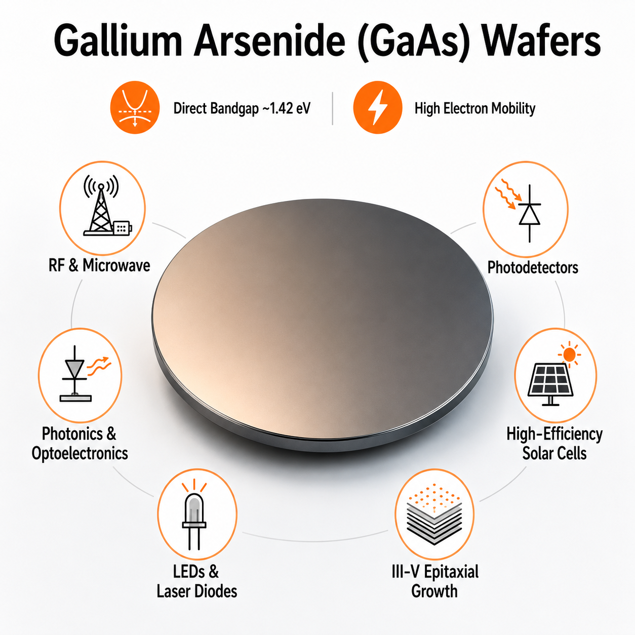
Gallium arsenide combines several properties that make it valuable for advanced semiconductor research. Compared with silicon, GaAs offers higher electron mobility and a direct bandgap, making it particularly suitable for high-frequency and optoelectronic devices.
- Direct bandgap: approximately 1.42 eV at room temperature
- High electron mobility for high-speed electronics
- Strong optical properties for light-emitting and detecting devices
- High-frequency performance for RF and microwave applications
- III-V epitaxy compatibility for advanced heterostructures
GaAs Substrate Options
Researchers can select GaAs substrates according to their experimental and fabrication requirements. Important options can include crystal orientation, wafer diameter, thickness, doping, resistivity, surface finish, and conductivity type.
Both semi-insulating GaAs and doped semiconducting GaAs substrates are used in research. Choosing the correct configuration is important for applications such as epitaxial growth, device fabrication, photonics, and electrical characterization.
Common GaAs Research Areas
- High-frequency RF and microwave devices
- LEDs and semiconductor lasers
- Photodetectors and optical sensors
- High-efficiency solar cells
- III-V epitaxial growth
- Quantum devices and nanostructures
- High-speed transistors
Need a Specific GaAs Wafer?
Tell us the diameter, orientation, thickness, doping, resistivity, and surface finish required for your research. We can help identify a Gallium Arsenide substrate that matches your project specifications.
Get Your Gallium Arsenide Wafer Quote FAST! Or Buy Online and Start Researching Today!
Why Use Gallium Arsenide (GaAs) Wafers?
Gallium Arsenide (GaAs) is a III-V compound semiconductor valued for its high electron mobility, direct bandgap, and excellent high-frequency performance. These properties make GaAs wafers especially useful for applications where conventional silicon substrates may not provide the required optical or electronic performance.
Because GaAs has a direct bandgap of approximately 1.42 eV at room temperature, it efficiently emits and absorbs light. This makes it an important substrate material for optoelectronics, photonics, LEDs, laser diodes, photodetectors, and high-efficiency photovoltaic research.
GaAs Wafer Applications
Gallium arsenide substrates are used throughout semiconductor research and advanced device development. Common applications include:
- RF and microwave electronics for high-frequency device research
- Laser diodes and LEDs for optoelectronic applications
- Photodetectors and optical sensing devices
- Solar cells and multi-junction photovoltaic research
- Photonics and integrated optical devices
- High-speed transistors and advanced semiconductor devices
- Epitaxial growth of III-V semiconductor structures
- Quantum and nanotechnology research
Selecting a GaAs Substrate
The appropriate GaAs wafer depends on the fabrication process and research objective. Important specifications to consider include wafer diameter, crystal orientation, thickness, conductivity, dopant, resistivity, surface finish, and grade.
GaAs substrates may be supplied as semi-insulating or semiconducting material depending on the application. Semi-insulating GaAs is particularly useful when electrical isolation is important, while doped substrates can be selected for electronic and optoelectronic device fabrication.
GaAs for Research and Device Development
Researchers use GaAs wafers to investigate next-generation semiconductor devices, high-frequency electronics, epitaxial thin films, optical components, and compound semiconductor heterostructures. Selecting the correct substrate specifications can help improve compatibility with deposition, lithography, etching, epitaxy, and device fabrication processes.
UniversityWafer can help researchers source Gallium Arsenide wafers with specifications suited to university, laboratory, prototype, and semiconductor research requirements.