
Why Choose Gallium Arsenide Wafers?
Gallium arsenide (GaAs) is a III-V compound semiconductor known for its high electron mobility, direct bandgap, and excellent high-frequency performance. Compared to silicon, GaAs enables faster electron transport and more efficient light emission, making it an ideal substrate for RF devices, microwave circuits, optoelectronics, and high-speed communications. Researchers and manufacturers worldwide rely on III-V semiconductor wafers to develop next-generation electronic and photonic technologies.
UniversityWafer supplies premium GaAs wafers grown using Vertical Gradient Freeze (VGF) and Liquid Encapsulated Czochralski (LEC) crystal growth methods. Our substrates are available in semi-insulating, undoped, and doped configurations with multiple wafer diameters, orientations, thicknesses, and polished surface finishes to meet the demanding requirements of research laboratories and commercial semiconductor production.
Typical Applications
- RF and microwave electronics
- Monolithic Microwave Integrated Circuits (MMICs)
- High Electron Mobility Transistors (HEMTs)
- Laser diodes and LEDs
- Photodetectors and optical sensors
- High-efficiency multi-junction solar cells
- Integrated photonics
- Satellite and aerospace electronics
- 5G and wireless communication devices
- University and government research
Available Specifications
UniversityWafer offers gallium arsenide substrates in a wide range of diameters, crystal orientations including (100) and (111), semi-insulating and conductive grades, epi-ready surfaces, single-side polished (SSP) and double-side polished (DSP) options, as well as custom specifications for advanced semiconductor and photonics research.
Get Your Gallium Arsenide Wafer Quote FAST!
Whether you need a single research wafer or production quantities, our experienced team can help you select the ideal GaAs substrate for your application. We offer competitive pricing, fast delivery, and custom wafer solutions.
Get Your Gallium Arsenide Wafer Quote FAST! Or Buy Online and Start Researching Today!
What Are Gallium Arsenide (GaAs) Wafers?
Gallium arsenide (GaAs) wafers are single-crystal substrates made from the compound semiconductor gallium arsenide, a material renowned for its direct bandgap, high electron mobility, and exceptional high-frequency performance. Unlike silicon, GaAs efficiently converts electrical energy into light, making it an ideal substrate for optoelectronic devices such as LEDs, laser diodes, and photodetectors. It also supports faster electron transport, enabling high-speed electronic devices used in telecommunications, aerospace, defense, and satellite systems.
GaAs crystals are commonly grown using Vertical Gradient Freeze (VGF) or Liquid Encapsulated Czochralski (LEC) methods to produce high-purity, low-defect substrates suitable for epitaxial growth and advanced semiconductor fabrication. UniversityWafer supplies semi-insulating, undoped, and doped GaAs wafers with a variety of diameters, crystal orientations, and polished surface finishes for both research and production.
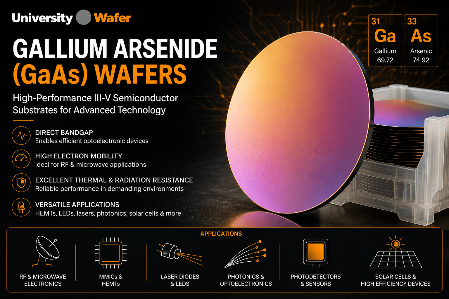
Key Properties of Gallium Arsenide
- Direct bandgap semiconductor for efficient light emission
- High electron mobility for ultra-fast electronic devices
- Excellent performance at microwave and millimeter-wave frequencies
- Lower electronic noise than many conventional semiconductor materials
- High radiation resistance for aerospace and satellite applications
- Suitable for epitaxial growth of complex III-V semiconductor structures
- Excellent thermal stability for demanding electronic environments
Applications of GaAs Wafers
Gallium arsenide wafers are widely used in photonics, RF electronics, microwave integrated circuits, high-speed transistors, laser diodes, LEDs, photodetectors, infrared devices, satellite communications, radar systems, high-efficiency multi-junction solar cells, and quantum research. Their unique electrical and optical properties make GaAs one of the most important materials in the III-V semiconductor industry.
Choosing the Right GaAs Wafer
Selecting the ideal gallium arsenide wafer depends on your device design, epitaxial growth requirements, conductivity type, crystal orientation, wafer diameter, surface finish, and intended application. UniversityWafer provides standard and custom GaAs substrates, including semi-insulating, n-type, and p-type wafers, with SSP, DSP, and epi-ready finishes to support semiconductor fabrication, photonics research, RF development, and advanced optoelectronic applications.