
Why Use GaAs for High-Efficiency Solar Cells?
Gallium arsenide (GaAs) is a III-V semiconductor widely used in advanced photovoltaic devices where high conversion efficiency, temperature stability, and radiation resistance are important. Its direct bandgap of approximately 1.42 eV at room temperature makes GaAs particularly well suited for converting sunlight into electrical energy.
Compared with conventional silicon photovoltaics, GaAs solar cells can achieve very high efficiencies while using relatively thin semiconductor layers. This combination makes the technology especially attractive for applications where power-to-weight ratio, available surface area, and long-term performance are critical.
Key Advantages of GaAs Solar Cells
- Direct bandgap – Efficient absorption of solar radiation allows comparatively thin active layers.
- High conversion efficiency – GaAs is a leading material for high-performance single-junction and multijunction photovoltaic devices.
- Radiation resistance – Useful for satellites and other space environments exposed to energetic particles.
- High-temperature performance – GaAs devices generally retain performance well under elevated operating temperatures.
- Multijunction compatibility – GaAs can be combined with other III-V semiconductor materials to capture a broader portion of the solar spectrum.
GaAs Wafers for Photovoltaic Research
High-quality GaAs wafers and substrates provide a crystalline platform for epitaxial growth and fabrication of advanced solar-cell structures. Researchers can use GaAs substrates for developing single-junction cells, tandem devices, multijunction architectures, and thin-film photovoltaic structures.
Depending on the device design, epitaxial layers may be grown using techniques such as metal-organic chemical vapor deposition (MOCVD) or molecular beam epitaxy (MBE). Precise control of layer thickness, composition, and doping enables researchers to engineer photovoltaic structures for specific wavelengths and performance requirements.
GaAs Solar Cells for Space Applications
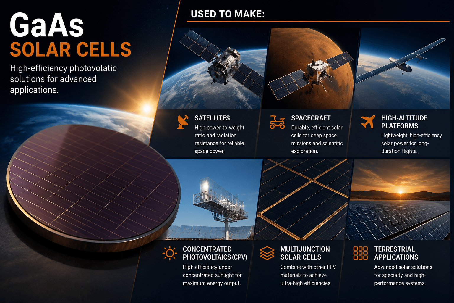
One of the most important applications for GaAs photovoltaics is space-based power generation. Satellites and spacecraft require solar cells capable of producing substantial electrical power while minimizing mass and maintaining performance in demanding radiation environments.
GaAs-based and III-V multijunction solar cells are commonly investigated for:
- Satellites and communications systems
- Scientific spacecraft
- Space-based sensors and instruments
- High-altitude platforms
- Concentrated photovoltaic systems
- Next-generation multijunction solar research
The combination of high efficiency, low mass potential, temperature tolerance, and radiation resistance makes GaAs an important semiconductor material for photovoltaic technologies where performance is more important than minimizing material cost.
Need GaAs wafers for photovoltaic research? Get your GaAs wafer quote FAST, or buy online and start researching today!
GaAs Solar Cell Structure and Fabrication
A typical GaAs solar cell consists of carefully engineered semiconductor layers designed to absorb incoming photons and convert their energy into electrical current. High-quality gallium arsenide wafers can provide the crystalline substrate required for epitaxial growth and advanced photovoltaic research.
Device structures may incorporate differently doped GaAs layers, window layers, contact layers, and anti-reflective coatings. Precise control of these layers is important for reducing optical and electrical losses while improving overall photovoltaic performance.
Single-Junction and Multijunction GaAs Cells
GaAs can be used in both single-junction and multijunction solar cells. In a single-junction device, the GaAs absorber converts a specific portion of the solar spectrum into electricity. Multijunction devices stack semiconductor materials with different bandgaps so that each junction captures a different portion of the spectrum.
This approach can significantly improve overall energy conversion efficiency and is especially important for space photovoltaics and concentrated photovoltaic systems. III-V materials such as GaAs, AlGaAs, GaInP, and related semiconductor alloys can be incorporated into advanced multijunction structures.
GaAs vs. Silicon Solar Cells
Both silicon wafers and GaAs substrates are important materials for photovoltaic research, but they offer different advantages. Silicon dominates terrestrial solar power because of its abundance, established manufacturing infrastructure, and comparatively low cost.
GaAs is generally more expensive to manufacture, but its direct bandgap, strong optical absorption, high efficiency potential, and radiation tolerance make it valuable when device performance is prioritized over substrate cost.
| Property | GaAs | Silicon |
|---|---|---|
| Semiconductor Type | III-V | Group IV |
| Bandgap | ~1.42 eV | ~1.12 eV |
| Bandgap Type | Direct | Indirect |
| Optical Absorption | Very High | Lower |
| Radiation Resistance | High | Moderate |
| Relative Material Cost | Higher | Lower |
| Common PV Applications | Space, multijunction and high-efficiency research | Terrestrial and large-scale solar power |
Research Applications for GaAs Photovoltaics
Researchers use GaAs substrates and epitaxial structures to investigate new approaches to photovoltaic efficiency, optical management, semiconductor interfaces, and device reliability. These studies can support both terrestrial and space-based energy technologies.
- High-efficiency single-junction solar cells
- III-V multijunction photovoltaic devices
- Space and satellite solar power
- Concentrated photovoltaic (CPV) systems
- Thin-film and lightweight solar cells
- Epitaxial semiconductor research
- Radiation-resistant photovoltaic devices
- Advanced optoelectronic structures
GaAs Substrates for Solar Cell Research
Substrate characteristics such as crystal orientation, thickness, surface finish, doping, conductivity, and defect density can influence epitaxial growth and subsequent device fabrication. Selecting an appropriate GaAs substrate is therefore an important step when developing experimental photovoltaic structures.
UniversityWafer supplies semiconductor substrates for researchers developing photovoltaic, optoelectronic, and III-V semiconductor devices. Researchers can select wafer specifications appropriate for epitaxial growth, device processing, characterization, and experimental solar-cell development.