
Silicon Epitaxial Wafers for Research
UniversityWafer supplies silicon epitaxial wafers (epi wafers) for semiconductor research, microelectronics, device fabrication, and advanced materials development. Epitaxial growth creates a high-quality crystalline silicon layer on a silicon substrate, allowing researchers to control important characteristics such as layer thickness, doping type, and resistivity.
Why Use Silicon Epitaxy?
Silicon epitaxy gives researchers greater control over the electrical and structural properties of the device layer than a standard bulk substrate. Silicon epi wafers are commonly used for:
- Semiconductor device fabrication and process development
- MOSFET and transistor research
- Power semiconductor and high-voltage device development
- MEMS and sensor fabrication
- Integrated circuits and microelectronics
- Doping, diffusion, and implantation studies
Custom Epitaxial Silicon Layers
Researchers can specify important epi-layer characteristics according to their experiment. Common requirements include epitaxial layer thickness, resistivity, dopant type, substrate orientation, wafer diameter, and surface finish. Both P-type and N-type silicon configurations may be available depending on the required specification.
Silicon Substrates for Device Fabrication
In addition to epitaxial wafers, researchers can explore silicon wafers and silicon-on-insulator (SOI) wafers for semiconductor fabrication, MEMS, sensors, and other advanced research applications.
Need Custom Silicon Epi Wafers?
Send us your required wafer diameter, epi thickness, conductivity type, resistivity, orientation, and quantity to help us identify the appropriate epitaxial silicon wafer for your research.
Get Your Silicon Epitaxial Wafer Quote FAST! Or Buy Online and Start Researching Today!
Silicon Epitaxy for Advanced Semiconductor Research
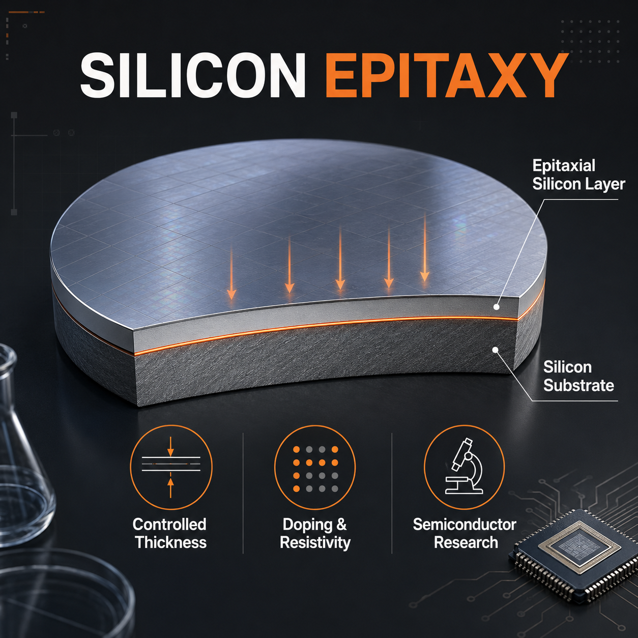
Silicon epitaxy enables researchers to grow a highly controlled single-crystal silicon layer on a silicon wafer. By selecting the epi-layer thickness, dopant, conductivity type, and resistivity, researchers can create substrates tailored for semiconductor devices, sensors, power electronics, and microelectronic research.
Epitaxial Silicon Layer Specifications
The properties of the silicon epitaxial layer can significantly influence device performance. Important specifications to consider when selecting an epi wafer include:
- Epi layer thickness – selected according to the intended device structure and process.
- Conductivity type – P-type or N-type configurations may be available.
- Dopant – commonly selected according to the required electrical characteristics.
- Resistivity – important for controlling the electrical behavior of the epitaxial layer.
- Crystal orientation – commonly specified for semiconductor processing and epitaxial growth.
- Wafer diameter and thickness – selected to match research equipment and fabrication requirements.
Applications for Silicon Epi Wafers
Silicon epi wafers support a broad range of semiconductor and materials research applications, including:
- MOSFET and transistor development
- Power semiconductor devices
- Integrated circuit research
- MEMS and microsensors
- Diodes and detector structures
- Doping and implantation studies
- Thin-film and interface research
Epitaxial Wafers and Alternative Silicon Platforms
The appropriate substrate depends on the required device architecture. Researchers can use conventional silicon wafers for general semiconductor processing or silicon-on-insulator (SOI) wafers when an electrically isolated device layer is required.
Epitaxy for Semiconductor Device Development
Controlled epitaxial layers give researchers additional flexibility when designing semiconductor structures. Silicon epitaxy is particularly valuable when the device layer must have electrical properties different from those of the underlying substrate.
UniversityWafer can help researchers source custom silicon epitaxial wafers based on wafer diameter, epi-layer thickness, doping, resistivity, orientation, surface finish, and quantity.