
Solar Cell Wafers for Research
Solar cell wafers provide the semiconductor foundation for photovoltaic (PV) devices that convert sunlight into electrical energy. UniversityWafer supplies substrates for university research, prototype development, material characterization, and next-generation solar cell experiments.
Silicon Wafers for Photovoltaics
Silicon wafers are widely used in photovoltaic research because of silicon's established semiconductor properties and compatibility with standard device fabrication processes. Researchers can select wafer characteristics such as conductivity type, resistivity, thickness, orientation, and surface finish to match their experiments.
P-Type and N-Type Silicon
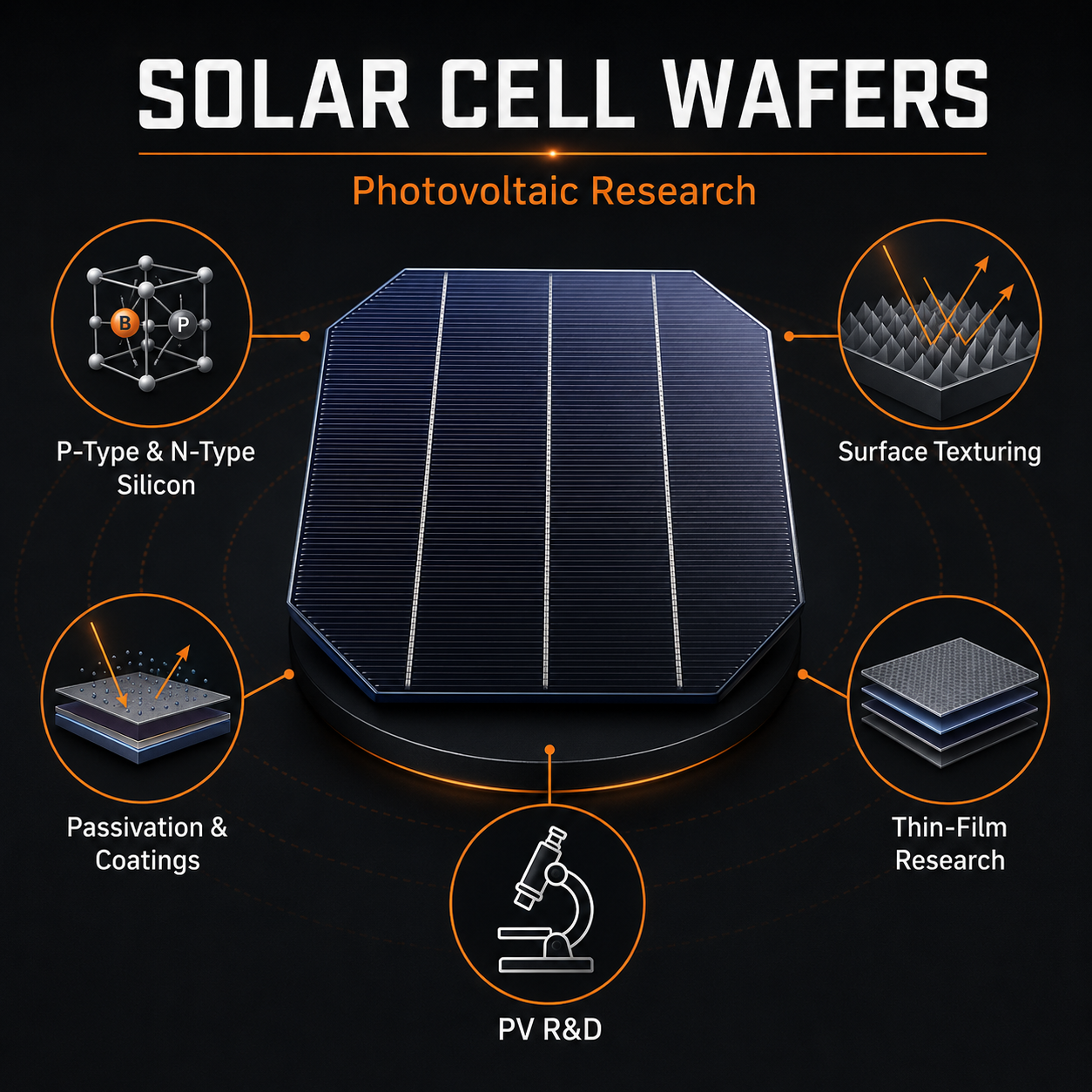
Both p-type and n-type silicon wafers can be used to investigate solar cell structures. The appropriate conductivity type and doping level depend on the device architecture, junction design, contact scheme, and research objectives.
Solar Cell Research Applications
- Silicon photovoltaic cell development
- Thin-film solar cell research
- Surface texturing and light trapping
- Anti-reflective coating studies
- Doping and junction formation
- Passivation layer research
- Metallization and electrical contacts
- Solar cell efficiency and performance testing
Surface Engineering for Solar Cells
Wafer surfaces can be modified to improve photovoltaic device performance. Research may involve surface texturing, passivation, thin-film deposition, anti-reflective coatings, and metallization. These processes allow researchers to investigate light absorption, carrier recombination, and electrical performance.
Choosing a Solar Cell Substrate
Important wafer specifications can include material, diameter, thickness, crystal orientation, conductivity type, resistivity, surface finish, and doping. Selecting appropriate specifications helps ensure compatibility with deposition, lithography, diffusion, etching, and other photovoltaic fabrication processes.
Need Wafers for Your Solar Cell Research?
Tell us your desired wafer material, diameter, thickness, conductivity type, resistivity, surface finish, quantity, and research application. UniversityWafer can help identify substrates suited to your photovoltaic experiments.
Get Your Solar Cell Wafer Quote FAST! Or Buy Online and Start Researching Today!
Why Use Silicon Wafers for Solar Cell Research?
Silicon wafers are a primary substrate for photovoltaic research because silicon offers well-understood semiconductor behavior, established processing methods, and compatibility with a wide range of solar cell architectures. Researchers can control doping, surface condition, resistivity, and thickness to investigate how wafer properties affect photovoltaic performance.
Monocrystalline Silicon Solar Cells
Monocrystalline silicon wafers provide a highly ordered crystal structure for studying photovoltaic devices. They are useful for investigating carrier transport, junction formation, surface passivation, light absorption, and other factors that influence solar cell efficiency.
P-Type vs. N-Type Solar Wafers
Both p-type and n-type silicon wafers are important in photovoltaic research. P-type substrates are commonly associated with traditional silicon solar cell architectures, while n-type substrates are widely studied for advanced structures designed to reduce recombination and improve device performance.
Surface Texturing and Light Trapping
Surface engineering can help a solar cell capture more incoming light. Researchers use surface texturing and light-trapping structures to reduce reflection and increase the optical path of light within the semiconductor, allowing more photons to contribute to photovoltaic conversion.
Passivation and Anti-Reflective Coatings
Silicon wafers can be used to study surface passivation and anti-reflective coatings. Materials such as silicon nitride (SiNx) and silicon dioxide (SiO2) are investigated for reducing surface recombination and managing optical reflection in photovoltaic devices.
Thin-Film and Next-Generation Photovoltaics
Wafer substrates are also useful for researching thin-film and advanced solar cell technologies. They can support deposited semiconductor, dielectric, and conductive layers for studying new device structures, interfaces, contacts, and photovoltaic materials.
Common Photovoltaic Research Areas
- Monocrystalline silicon solar cells
- P-type and n-type photovoltaic devices
- Surface texturing and light trapping
- Passivation and anti-reflective coatings
- Thin-film deposition
- Doping and junction formation
- Metallization and electrical contacts
- Solar cell efficiency characterization
- Next-generation photovoltaic structures
Selecting Wafers for Photovoltaic Experiments
Researchers should consider wafer material, crystal orientation, diameter, thickness, conductivity type, doping, resistivity, and surface finish. Requirements can vary significantly depending on whether the wafer will be used for device fabrication, coating experiments, surface modification, or electrical and optical characterization.
Solar Cell Wafers for R&D
UniversityWafer supplies silicon wafers and research substrates for photovoltaic R&D, including university research, prototype solar cells, materials studies, and process development. Specifications can be selected to match the requirements of your particular photovoltaic experiment.