Photovoltaic Technology- Silicon Wafers
Thin Silicon Wafers for Integrated Photovoltaics
We have thin silicon wafers that scientists use for their research. Please end us your specs or ask for our inventory today.
Get Your Quote FAST!
How to Build with Integrated Photovoltaics
Video on what the future holds for integrated photovoltaics.
What Are Solar Photovoltaic Cells Made Up Of?
The solar panel is a device that consists of several layers of solar cells. The front layer has a thin layer of glass that faces the sun. The backsheet is made of durable polymer-based material that prevents water from penetrating the cell. The solar cells are connected to the receiver of the produced current by electrical contacts. They also contain a junction box where the electrical connections are made inside the module. There is also a frame that protects the cell from impacts.
There are different types of solar cells. The single-crystal silicon cell is the most common and represents more than 95% of solar modules sold today. Silicon is the second most abundant element on earth after oxygen. It is also the most common material used in computer chips. The crystalline silicon cell is made of silicon atoms that are interconnected to form a crystal lattice. This structure makes the conversion of light into electricity more efficient.
There are many different types of solar cells. One type is called a single-crystal silicon cell. The other type is called a crystalline silicon cell. Both types have the same structure, but some are different from each other. The crystalline silicon cells are made of silicon atoms arranged in a hexagonal lattice. The hexagonal lattice has a higher ion density than the n-type silicon cells.
The solar cells are made of crystalline silicon boules. The atomic structure of one crystal is polycrystalline. To create the boules, the simplest way is to melt a polycrystalline silicon in a vacuum. The wax covered cells are then rotated to form a cylindrical ingot. The resulting material is a pure semiconductor that converts sunlight into electricity. It is the crystalline silicon that allows the panels to store electricity.
The solar cell is made of special materials called semiconductors. One of these is silicon. A photovoltaic cell works by absorbing light and transferring that energy to a material. The electrons on one side of the semiconductor move into the holes on the other side. This energy is converted to electricity in the semiconductor. Then, the light from the sun is converted into usable energy. This is a form of electricity.
To work, photovoltaic cells need an electric and magnetic field. These fields are caused when two opposite charges are separated. Then, the silicon sandwich is covered in other materials. The n-type silicon is covered by a thin layer of wax, while the p-type is coated with a thin layer of polyethylene terephthalate. A second type of semiconductor is a conductive material called a conductor.
There are several types of solar cells. Typical solar cells are made from crystalline silicon. In a solar cell, a p-type silicon atom is placed next to an n-type silicon atom. A p-type silicon molecule contains positively charged holes and negatively charged electrons. The resulting combination of these two substances makes a PV cell. However, adding solar panels to an existing home can be expensive and inefficient.
There are several types of solar cells. The most common type is a single-crystal silicon cell. These solar cells are made up of special materials called semiconductors. These materials can be monocrystalline or multicrystalline. Most solar cells are made up of a single-crystal silicon cell, which is the most common type. They are also used for making batteries. The technology used to manufacture these products is incredibly complicated.
When a solar cell is made, it consists of silicon boules. Silicon boules are polycrystalline structures with the atomic structure of a single crystal. During the manufacturing process of a solar cell, the silicon atoms are connected in a network, or crystal lattice. This helps the silicon cells convert light into electricity. The n-type silicon is the most expensive.
What are Integrated Photovoltaics?
Integrated photovoltaics are a new and innovative way to use solar power in buildings. They are made up of photovoltaic materials that can be incorporated into the building. These solar panels can be used in place of traditional building materials like skylights and roofs. They can even be built into the facade of a building. Here's how they work: - The materials are used to cover conventional building components.
When used in construction, photovoltaic systems have two primary functions. One is to collect energy from the sun, while the other serves a dual purpose. In BIPV, solar cells serve a dual purpose. They collect light and store it into electricity. They can be installed in any direction and still generate electricity. These systems have an efficiency of up to 90%. And they can be designed in almost any shape and size.
 Another type of BIPV is made of standard building materials combined with efficient photovoltaic elements. The demand for these solar products is expected to continue to grow in the 21st century. In 2011, NREL said that BIPVs would eventually overtake conventional photovoltaics. Today, with continued integration, solar products are becoming as widespread as traditional building materials. This is a major breakthrough for sustainable and affordable energy.
Despite the many benefits of using solar cells, integrated photovoltaics poses several challenges. For one, the building is often not accessible. This creates access problems. It also causes buildup of heat and can be difficult to align the solar modules in the most optimal way. Furthermore, the building must meet all national building codes and constructional standards. So far, these advantages are not outweighed by any drawbacks of this technology.
As a result, there is a need to address issues such as cost and design intent when integrating a solar cell into an architectural structure. The solar cell system needs to comply with the architectural integration requirements while meeting PV technologies and requirements. Additionally, the solar cells and their assembly methods must be compatible with the architectural design intent. It's not enough to simply incorporate the system in an existing structure. The building must also be environmentally conscious.
As an alternative to installing a solar panel on a roof, building-integrated photovoltaics (BIPV) have many other advantages. They are cheap and convenient. The technology is also becoming more sophisticated. The materials used for these panels are highly efficient and have low maintenance. In addition to being inexpensive, they also reduce the risk of fire. Some researchers are developing TPVs that can be integrated into existing buildings.
Integrated photovoltaics are a great option for buildings. They serve as the outer layer of a structure, generating electricity, reducing pollution, and enhancing architectural appeal. Although they are often installed as retrofits, the best results are achieved when PV systems are built into the structure from the beginning. By incorporating solar panels into a building's design, it can be much less expensive than installing them on a roof.
Integrated photovoltaics are used as part of a building and can be a primary source of electricity. These systems are also more eco-friendly because they reduce the need for traditional electrical power. Unlike traditional PV panels, they are also aesthetically pleasing. In addition to their utility benefits, BIPVs are cost-effective and can reduce building labor and material costs. Further, they are a great way to save money and the environment!
BIPV modules are an example of building-integrated photovoltaics. These modules are photovoltaics that can replace conventional building materials. They are also the main source of electricity for many buildings. They can reduce construction costs and labor costs and are a growing segment of the photovoltaic industry. When installed properly, BIPVs can be a great option for buildings of all types.
Integrated photovoltaics are the most popular form of PV systems, and they are becoming more popular in residential buildings. These PV modules are transparent and are added as an integral part of the building's roof. They can be added to a flat or tilted roof. They are generally added to small buildings. They can also be added to the walls of a building. The PV modules can be integrated into the glass or panels.
What is Macroporous Silicon?
Macroporous Silicon is a promising alternative material for photovoltaic devices. In this article, we review the 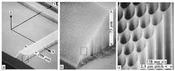 key characteristics of this material, including Optical generation, Photocurrent dependence on ITO coverage, and Photovoltaic characteristics. We also discuss the challenges of designing this material and evaluating its applications. You can download the article here. Read on to learn more! Posted on June 14, 2011 by macroporous silicon
Optical Generation
In this study, we investigated the effect of the conformal coating quality on the photocurrent and dark (dotted) lines of the optical devices. We studied the effect of pore density on the photocurrent at a 20 mm depth in a 3D macroporous silicon structure, using a Keithley 2400 source meter. Our simulations suggest that the pore density of the silicon layer is critical for achieving high photocurrent.
Macroporous silicon can be made using two-dimensional structures with different nanocoatings. Nanocoatings can increase the photoconductivity and electromagnetic radiation absorption of the silicon material. The two-dimensional structures with nanocoatings can be used for photovoltaic systems and solar cells. The energy-conversion efficiency can be increased up to 60%. Another major advantage of macroporous silicon with nanocoatings is that they can be used in the upper atmosphere and field.
Electrochemical etching of silicon using macroporous structures involves an ion-exchange process. The silicon surface is exposed to HF ions, resulting in electron-hole formation. At higher illumination intensities, the silicon molecules undergo a chemical reaction with fluorine ions. Electrochemical etching requires tuning of the process parameters. Furthermore, prolonged etching may lead to unstable pore formation.
In order to determine the pore depth, we used a pn-Si device that had a pore depth of 440 mm. The photocurrent measured at different depths was correlated with the pore length. Our simulations showed that the photocurrent can be increased by improving the ITO coverage along the pore depth. The resulting device exhibits the photocurrent dependence of ITO coverage.
Photocurrent Dependence on ITO Coverage
The photocurrent dependence on ITO coverage of macropores in a n-type substrate is largely dependent on the electrochemical parameters: the current density and the potential. For example, under potentiostatic control, a 15-mm pitch macropore array etched at 3.5 V/CE and 140 W illumination yielded nearly perfect edges, but the photogeneration at the edge was poor.
Using the oCVD PEDOT/planar-Si recombination process, a high-doped composite CdTe/PEDOT/PSS device was fabricated with a photocurrent of twenty-four uA at -1 V. This was nearly three times higher than the corresponding values for HC-PEDOT-PSS/planar-Si devices.
In Figure 3c, the photocurrent is sufficiently high for a high voltage. In contrast, the photocurrent is too high in the edges, causing the pore formation to become unstable. The resulting photocurrent is spatially homogeneous. For these reasons, photocurrent on an ITO-coated silicon substrate should be a consideration in designing a device. Further, it will help improve the understanding of how a semiconductor device works.
The engineering pore dimension of b-Si has been optimized to yield a mode-tunable Si photodetector. The bias polarity of the photodetector can be switched between visible-blinded and broad-band modes. This feature opens the door for novel sensing platforms. If this technique can be reproduced at the nanoscale, it could become an important part of a wide range of future sensor designs.
In addition to this, the photocurrent-dependent ITO coverage in macroporeous silicon can be improved by making the morphology of the pores more uniform. ITO masks are compatible with the photolithographic process, and the removal techniques must not negatively impact the PoSi. A well-designed mask can be used to achieve the desired photocurrent dependence. So far, silicon electrochemical etching is a low-cost and highly reliable method for creating large areas of porous silicon.
Photogeneration Rate Along Pore Surface
The photogeneration rate along the pore surface of macroporous silicon is highly dependent on the etching parameters. This is particularly important in the microelectronics industry, where n-type silicon electrodes with a resistivity of a few O cm are common. Below these boundary values, competition for the holes is high and silicon dissolution proceeds with the formation of pits at defect sites. As a result, the photogenerated hole collection is no longer uniform; some pits collect more holes than others.
Generation is calculated as the difference between the amplitude and the total amount of incoming light. The light intensity decreases exponentially along the pore surface, while generation at the surface is the highest. Because incident light has multiple wavelengths, the generation rate varies according to its wavelength. To study the generation rate along the pore surface of macroporous silicon, we first consider the cone-shaped pore morphology of the macropore.
Using simulated photocurrents, we have characterized the photogeneration rate along the pore surface of macroporous silicon. A larger pore depth results in higher photocurrent in pn-Si devices. In addition, photocurrent varies with the ITO coverage along the pore wall. Photocurrents measured at this depth were highly dependent on the pore depth. We have compared photocurrent dependence of different pore depths with pn-Si devices using the same ITO electrode.
While it is important to understand the effect of pore-wall roughness on photogeneration rate, little research has been done on the matter. The study by E. Foca and co-authors reveals that smoothing the pore wall during etching can reduce the surface reflectance to less than 5% over the VIS-NIR region. It also outperforms state-of-the-art techniques.
Photovoltaic Characteristics
The boron emitter, phosphorus dopant, and well-defined structural properties of macroporous silicon make them attractive candidates for use in photovoltaic devices. The pore walls of macroporous silicon are highly porous, so that light can penetrate through them easily. The front side of the monocrystalline silicon layer contains a single D2diode. The rear side of the monocrystalline silicon layer contains two D3diodes, one located at the back end.
The photocurrent values in a PS/Ox/FTO heterojunction show a linear dependence on light intensity. In contrast, D1 exhibits a 2,000-fold higher photocurrent density than D2. This is consistent with the fact that D1 is more sensitive to light than D2, which indicates that it can withstand higher amounts of illumination. In addition, the reverse bias region is only significantly modified when the light intensity increases.
Microfluidic Applications
Macroporous silicon can be used for microfluidic devices, including microfluidic pumps and sensors. The process of making macropores involves the formation of highly ordered layers of macropores. These structures are made using a process called electrochemical etching. Various chemical processes are used to produce macropores. This article will describe one of these methods. It will be useful in the design of microfluidic devices.
In order to fabricate microfluidic devices, n-type macroporous silicon is fabricated and patterned. This enables the formation of a pn-Si junction. After a spin-on-dopant (SOD) process, a layer of Borofilm 100 is used to form the p-layer. The p-layer is then diffused in a nitrogen atmosphere.
The synthesis and design of macroporous silicon using a high-aspect ratio is explored in this article. The article also discusses potential applications of macroporous silicon. This novel material offers many benefits for microfluidic applications and is expected to continue to garner interest. Its properties make it a promising candidate for microfluidic devices, including sensors and actuators. In addition to these applications, it is also an excellent material for a variety of other types of materials.
Another microfluidic application of macroporous silicon is as a filter for particles. It is difficult to integrate a filter with a downward opening, but diaphragms made of macroporous silicon have a cavity beneath them. The cavity can then be used to place sensor components. One German patent application describes a diaphragm sensor unit with a microporous cavity. Another application is thermal isolation.
Video: Fabricating Porous Silicon
Are Photovoltaic Cells Waterproof?
Are photovoltaic cells waterproof? Yes, they are waterproof by design. These solar cells can survive a hail storm, a wash, or even submersion. But how do you protect your panels from damage from water? Here's what you need to know. The best solar panels are sealed to prevent water from entering the cells and wiring. Read on to learn more. And if you have any questions, feel free to contact us.
Solar panels are waterproof by design
Solar panels are waterproof by design. They are constructed of glass sheets that are sealed within a metal  frame. The frame is made to prevent water from damaging the PV cells and wiring inside the panel. The panels are installed permanently at an angle that maximizes sunlight capture while preventing water damage. To achieve this, the panels must be tested in extreme weather conditions, including humidity and freezing temperatures. Water pressure and leakage are also factors that should be taken into consideration.
Generally, solar panels and photovoltaic cells are designed to withstand the effects of snow and rain. They are durable and waterproof and can withstand considerable weight without collapsing. This means that users in colder climates need not worry about heavy snow damaging their solar panels. They also benefit from snow and rain. They can generate electricity even when the power grid is down due to bad weather.
The solar cell can withstand laundry. Researchers from the Japanese research institute RIKEN developed a waterproof cell made of PNTz4T. The researchers deposited this device using inverse architecture on a parylene film. The new waterproof cell can survive washing and allows sunlight to reach the cells. This waterproof cell can be used to power wearable devices such as sensors. They can even be a part of a solar-powered car.
When installed properly, solar panels are waterproof. The glass sheets protect the PV cells from water. Installers usually mount them at an angle that allows water to roll off the panels and make them self-cleaning. The glass sheets may become dusty over time, reducing the amount of sunlight that they receive. Regardless of whether they are waterproof, it's important to check with the manufacturer of your solar panel to make sure that they are covered by a warranty.
Can You Wash Solar Panels?
Researchers have developed a new type of photovoltaic cell that is washable and can be streched by half. The PNTz4T material used to create the device is deposited in an inverse structure onto a parylene film. This enables the cell to be washed and dried, and the scientists say it is twice as efficient as the thinnest solar battery.
The new solar cell combines three key characteristics of photovoltaic technology - a high energy density, stretchability, and stability in both air and water. Developed by Takimiya's group, it is capable of converting sunlight into electricity with nearly eight per cent efficiency. The organic photovoltaic material is 1 micrometer thick and is stable even under water and air. The thin OPVs were tested under mild conditions.
Can Solar Panels Withstand a Hail Storm?
The question of whether photovoltaic cells can withstand a harsh hail storm is a legitimate one. Hail, a solid form of ice, is created when the moisture in the air is pushed upward during a storm's updraft. This combines hot and cold temperatures to form hailstones. Big hailstones are particularly destructive during a storm, as they are extremely fast and can cause serious damage to solar panels.
The solar panels on which your solar panels are installed are typically covered in tempered glass. They are typically mounted at an angle to deflect hail, a slightly higher risk for damage than a flat panel. However, solar panels mounted at an angle of 10 degrees or less still stand a good chance of surviving a hailstorm. So, yes, photovoltaic cells can withstand a hail storm if they are installed in a sheltered area.
Although hail damage can result in significant financial losses, the technology is available to minimize damage. It's a great help if you're considering installing a solar energy array in a hail-prone area. The next step in mitigating hail damage is to install a tracker. NEXTracker's NX Navigator hail protection module allows you to move the entire solar array to a safe 60-degree stow angle.
While hail damage does occur during storms, most solar warranties don't cover it. Some warranty policies cover hailstorm damage as part of their coverage for other environmental factors. Check to see how comprehensive your policy is and if you're covered for hailstorm damage. Otherwise, it's best to get your solar panel installed by a professional. Otherwise, you risk getting shocked and voiding your warranty.
The testing procedures for PV modules were not designed with the other states in mind. NASA's Jet Propulsion Lab advised developers in the Great Plains to prepare for a hailstorm with hailstones as large as 38mm. This is 50 percent larger than the current testing standards. The hailstones that hit the building tended to be concentrated. However, the hailstones themselves were too large to destroy the solar modules.
Can you Submerge Solar Panels in Water?
The electrical characteristics of Photovoltaic cells and modules are evaluated for different depths of submersion. This standard testing procedure is based on the electrical circuit diagram shown in Fig. 1(a). A variable rheostat, a DC voltmeter, and a current meter are used to measure the voltage and current of the SPV module in two and twelve centimeters of water.
The efficiency of solar cells can be increased by about 15% during summer and around 5% year-round. The water can also cool the cell surface and remove dust that accumulates on its surface. The water's effect on the solar cells is beneficial because it can refract sunlight, which increases the output of the cells. Therefore, if you're thinking of using a solar panel to generate electricity, this is a good option.
However, the depth of water affects the efficiency of the PV cells. For instance, the deepest depth of water reduces the surface temperature of a PV cell, thereby increasing its electrical efficiency. In a test, the maximum electrical efficiency of a SPV was recorded at one centimeter of water, and it increased by 17.8% as compared to its surface temperature.
Underwater photovoltaics are already being used in various applications. These applications range from power generation and energy storage to underwater monitoring of bridges and underwater tunnels. These cells can also be used for various purposes including salt farming, marine exploration, and desalination. This new technology has a bright future. With the right application and development, it could become a mainstream renewable energy source.
Video: Waterproof Solar Panels
Five Development Trends of Photovoltaic High-Frequency Inverters
As the use of solar energy increases globally, so does the demand for photovoltaic high-frequency inverter technology. Several trends are influencing this technology, including the need for better boosting and more detailed sensing. More efficient designs and earlier warning algorithms are also vital to the consistent production of solar energy. The five development trends outlined below are set to further accelerate the development of photovoltaic high-frequency inverter technology.

Boosting is required
Photovoltaic high-frequency inverters must be isolated from the grid to avoid leakage currents. A transformer-less inverter has no transformer-isolation between the PV panel and the ac grid, so leakage currents may be large. The injected dc component can overload distribution transformers. Most safety standards for grid-tied inverters limit the injected dc current. Some models, however, do not include transformer isolation.
The main disadvantage of boost units is that they cannot operate without active switches. These devices are prone to reverse-recovery problems. However, they are a great alternative to conventional high-frequency inverters. It is possible to minimize the number of PV inverters by connecting them in series. However, this can be expensive. For this reason, many PV inverters require boosting.
The Boosting module can be connected in parallel to the dc source. This topology can be extended to "n" modules. Each module has two diodes and a capacitor. All capacitors are charged to a constant level, NLevel. The boosting module's output voltage is derived by NLevel, Ndiode, and NCapacitors. As the number of modules increases, the voltage gain also increases.
A common design of photovoltaic high-frequency inverter is a buck-boost configuration. This configuration uses an embedded boost converter with a fixed duty cycle of 50 percent. An active switch is placed on the input side of the converter, which further increases the volume. This configuration also involves diodes on the load side of the converter. There is a lot of room for improvement in photovoltaic high-frequency inverters and their efficiency.
Sensors require more detailed sensing
Inverters that use a DC-to-AC converter need current sensors to measure the DC component of grid current. These sensors must meet specific requirements from the utility system, including synchronization and low total harmonic distortion. Inverters also need current sensors to control the inverter's control loops, ensuring proper connections to the utility grid. These sensors must also be highly accurate and have low offset drift with temperature.
Current-to-current measurement is required for the MPPT control phase of a DC PV inverter, which maximizes power generation efficiency. Overcurrent detection is needed to identify a short circuit and detect a failure of a PV panel. High sensitivity, low sensitivity drift, and fast response are important characteristics of the current-to-voltage converter.
Light-sensitive photovoltaic inverters typically use photodiodes or silicon controlled rectifiers. These devices are PN-junction devices that respond to light by generating an output signal. Light sensors are also commonly used in cameras, light meters, and TV remote controls. A phototransistor, which works by converting light energy into electricity, is essentially a PN-junction light sensor.
Product types require more diversified design
More diversified design of photovoltaic high frequency inverters is needed for various products, including thin-film PV panel solutions. Inverters are able to adapt to different power grids. However, there are still many challenges associated with them. This article discusses some of these challenges. We will also discuss some of the solutions for the same. The first solution involves installing a frequency transformer on the output end. The frequency transformer's primary is not grounded. A "Y"-type connection is recommended, and the inverter is connected to a protective ground.
Another way to improve the design of inverters is to use different materials and structures. Different materials have different characteristics and require different inverter configurations. Moreover, BIPV projects require more diverse designs for safety, aesthetics, and operation. The followings will provide some guidelines for selecting the right inverter for your BIPV project. They are an important part of solar power technology.
Photovoltaic high-frequency inverters are increasingly used in distributed systems. Distributed systems are the future of photovoltaic power generation. With increased policies, they will grow rapidly. Distributed photovoltaic power stations will become the norm, while new applications, such as floating photovoltaics, will continue to grow. As these developments unfold, photovoltaic high-frequency inverters will need to reflect these factors and be more scientifically designed to achieve maximum efficiency.
String inverters are more efficient
The efficiency of string high-frequency inverters has been continuously improved, with the maximum capacity now reaching 80 KW. Its weight has decreased, too, and its design adapts to a complex application environment. The Sungrow 40KW string inverter is now the lightest product of its kind in the industry, weighing just 39 kg. The inverter's intelligent fan has been proven to be highly effective in reducing the temperature of its internal components and ensuring overload capacity in high temperature environments.
The string type of high-frequency inverters are used for solar installations, and their efficiency is increasing as improvements in semiconductor technology have been made. String inverters can now have power densities of tens to hundreds of kW, with their modular design making maintenance simple. As their capacity increases, the cost of replacing them is low. String high-frequency inverters are also more affordable than their equivalent centralized residential counterparts, with standard warranties lasting between five and ten years. Some companies offer maintenance and monitoring services as part of their solar contracts.
The string high-frequency inverters are more efficient than their predecessors thanks to their improved switching characteristics. The string high-frequency inverters feature bidirectional switching capability, which increases efficiency. Unlike traditional three-phase H-bridge inverters, these are bidirectional. Their bidirectional switching capability allows them to charge batteries when needed, a feature of standard string inverters. And because they are more efficient, they can be used in large-scale solar installations, such as on a rooftop.
FIT rates are not currently offered
Recent policy announcements and the impending revisions to Vietnam's feed-in tariff program have many investors hopeful that the PV market in the country will finally reach its full potential. Although the FIT program is primarily intended for utility-scale and commercial rooftop PV, tremendous developer activity is already underway under the current regime. EVN, the state-owned power company in Vietnam, is attempting to balance the need to build solar power with costs and capacity. The country has placed strict caps on project capacities.
FIT rates for photovoltaic high frequency inverters are not currently offered in the United States, but it could be available soon. The solar industry is eager to move forward with grid parity and is hoping that most regions of the world can achieve grid parity by 2020. To achieve grid parity, FIT rates must be lower than current levels and the PV industry must address climate change in order to remain competitive. Huawei is currently pursuing the development of artificial intelligence to accelerate grid parity.
Long-standing grid constraints are another issue
PV inverters need a flexible power control strategy to perform multiple functions. Such flexible power control strategies enable PV systems to integrate more seamlessly with the grid. Several experimental case studies have demonstrated the flexibility of PV inverters in performing multiple functions. However, grid-connected PV inverters face long-standing grid constraints. These constraints are also another obstacle to the deployment of PV systems.
A recent report from the International Energy Agency argues that the long-term viability of PV high-frequency inverters relies on their ability to support voltage recovery. This capability is required for grid-connected PV systems to support the grid during voltage faults. In Fig. 4b, the reactive current required by medium and high-voltage PV systems is shown.
Another problem is transformer-less PV inverters. The transformer-less PV inverters must account for common mode leakage current. However, this problem is largely a design issue, and will need to be addressed before commercial PV inverters become widely available. Long-standing grid constraints may also pose a challenge to the future of PV high-frequency inverters.
One solution is to agree on a maximum voltage for solar panels, which is currently at approximately 80%. This would prevent any over-voltage events, which would cause increased grid voltage and short-circuiting of the PV system. Another solution is to unlock the inverter. This unlocking of the PV system will make it possible for the inverter to be adjusted to improve grid management.