Do you also have ITO deposited glass and FTO deposited glass?
If yes, I need 1/2 inch by 1/2 inch around 500 pieces.
Fluorine-doped Tin Oxide (FTO) Substrate
FTO Deposited Glass Wafers
A postdoc requested a quote for the follwoing.
UniversityWafer, Inc. Quoted:
FTO Glass Substrate (TEC 15) 1" x 1" x 2.2 mm, R:12-14 ohm/sq
ITO Coated Glass Substrate 10mm x 10 mm x 0.7 mm, R:9-15 ohm/sq,Nominal ITO film thickness: 180 nm
Reference #139874 for specs and pricing.
FTO Conductive Transparent Substrates
A PhD candidate requested a quote for the following.
The dimensions don't really matter to me. I just need conductive, transparent substrates that will be diced into pieces ranging from 1cm x 1cm to approx. 1" x 2". The thickness is not really important either, just thick enough that they can be handled easily without breaking, maybe around 1 mm. It
It doesn't specifically have to be ITO/FTO as I specified, it just needs to be high conductivity, highly transparent and be chemically stable in mild acid and base solutions for durations of up to maybe a day.
Reference #103101 for specs and pricing.
Get Your FAST! Or, Buy Online and Start Researching Today!
What are FTO Substrates and What are its Semiconductor Applications?
FTO Substrates refer to Fluorine-doped Tin Oxide coated glass.
-
FTO stands for Fluorine-doped Tin Oxide (SnO₂:F).
-
It’s a transparent conducting oxide (TCO) — meaning it allows light to pass through while also
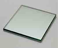 conducting electricity.
 -
Typically, it’s a thin film of tin oxide (SnO₂) that's doped (i.e., intentionally modified) with a small amount of fluorine to improve its electrical conductivity without significantly sacrificing transparency.
- The substrate usually refers to the underlying material — most often glass, sometimes plastic or other surfaces.
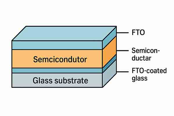
Why FTO is special:
-
It’s highly transparent (~80% or more in visible range).
-
It’s chemically stable (better than Indium Tin Oxide, or ITO, in harsh conditions).
-
It’s conductive with relatively low sheet resistance (typical: 10–20 ohms/sq).
-
It tolerates high processing temperatures (>500°C), which is important for certain semiconductor fabrication steps.
Applications of FTO Substrates in Semiconductors:
| Application | Role of FTO Substrate | Why FTO is used | Image |
|---|---|---|---|
| Solar cells (Dye-Sensitized Solar Cells, DSSCs) | Acts as the transparent electrode where photoelectric conversion happens. | High transparency + electrical conductivity. | 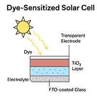 |
| Perovskite Solar Cells | Front electrode and sometimes as a bottom substrate for spin-coating layers. | Stability against halides and processing temperatures. | 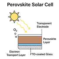 |
| Photocatalysis (e.g., water splitting) | Conductive support for photocatalyst layers like TiO₂. | Chemically stable in aqueous and oxidative environments. | 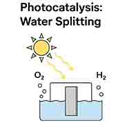 |
| Electrochromic devices (smart windows) | Conductive layer where voltage changes optical properties. | Durability under cycling. | 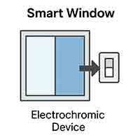 |
| Sensors | Base layer for biosensors, gas sensors, etc., for electrochemical or photoelectrochemical detection. | Good combination of transparency, conductivity, and chemical inertness. | 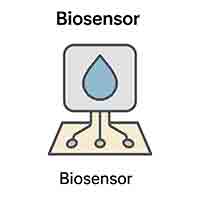 |
| OLEDs / Displays | Alternative transparent anode in displays when stability matters. | When stability is more critical than conductivity. |  |
Quick real-world example:
In a dye-sensitized solar cell, you have a sandwich structure:
Glass → FTO → TiO₂ layer → Dye → Electrolyte → Counter electrode
Here, the FTO provides both the light entrance path and the electric contact to collect generated charges.
