
Gallium Nitride Wafers for Research
Gallium Nitride (GaN) is a wide-bandgap semiconductor that supports research into devices operating at high power, high frequency, and elevated temperatures. Its electronic and optical properties have made GaN an important material for next-generation power electronics, RF technology, optoelectronics, and photonics.
UniversityWafer supplies GaN wafers and epitaxial substrates for university laboratories, industrial R&D, process development, material characterization, and experimental semiconductor device fabrication.
Why Researchers Choose GaN
Compared with conventional silicon, GaN provides material properties that are attractive for demanding semiconductor applications. Its wide bandgap and high critical electric field support high-voltage operation, while its electronic properties make GaN valuable for high-frequency devices.
- Wide bandgap of approximately 3.4 eV
- High critical electric field
- High electron mobility
- High-frequency device capability
- High-temperature research applications
- Direct bandgap for optoelectronic applications
GaN Substrate Platforms
GaN can be supplied as bulk or freestanding material and as epitaxial layers grown on other semiconductor substrates. The appropriate platform depends on the device architecture, thermal requirements, research objectives, and fabrication process.
- Bulk and Freestanding GaN – useful when researchers require a native GaN substrate.
- GaN on Silicon (GaN-on-Si) – combines GaN device layers with established silicon wafer technology.
- GaN on Silicon Carbide (GaN-on-SiC) – widely investigated for demanding RF and power applications.
- GaN on Sapphire – commonly used for LED, optical, and semiconductor research.
GaN Wafer Specifications to Consider
Researchers should select a GaN wafer according to the requirements of their experiment. Important specifications can include:
- Wafer diameter
- Substrate material
- GaN layer thickness
- Conductivity and doping
- Crystal orientation
- Surface finish
- Epitaxial layer structure
- Dislocation and defect requirements
GaN HEMT Research
One important area of GaN research involves High Electron Mobility Transistors (HEMTs). GaN-based heterostructures can support high carrier densities and high-speed operation, making them valuable for power conversion, RF amplifiers, microwave electronics, and communications research.
Researchers can use GaN HEMT structures to investigate breakdown behavior, switching performance, device reliability, interface properties, and advanced transistor designs.
GaN for LEDs and Optoelectronics
Because GaN is a direct-bandgap semiconductor, it is also an important material for light-emitting and optical devices. GaN-based materials are investigated for LEDs, laser diodes, photodetectors, ultraviolet devices, and other photonic technologies.
Epitaxial GaN structures allow researchers to investigate layer thickness, doping, interfaces, defects, and optical performance for experimental optoelectronic devices.
Need a Specific GaN Wafer?
Send UniversityWafer your required diameter, substrate, GaN thickness, doping, orientation, surface finish, and epitaxial structure. We can help identify an appropriate Gallium Nitride wafer for your research or process-development project.
Get Your Gallium Nitride (GaN) Wafer Quote FAST! Or Buy Online and Start Researching Today!
What Are Gallium Nitride (GaN) Wafers?
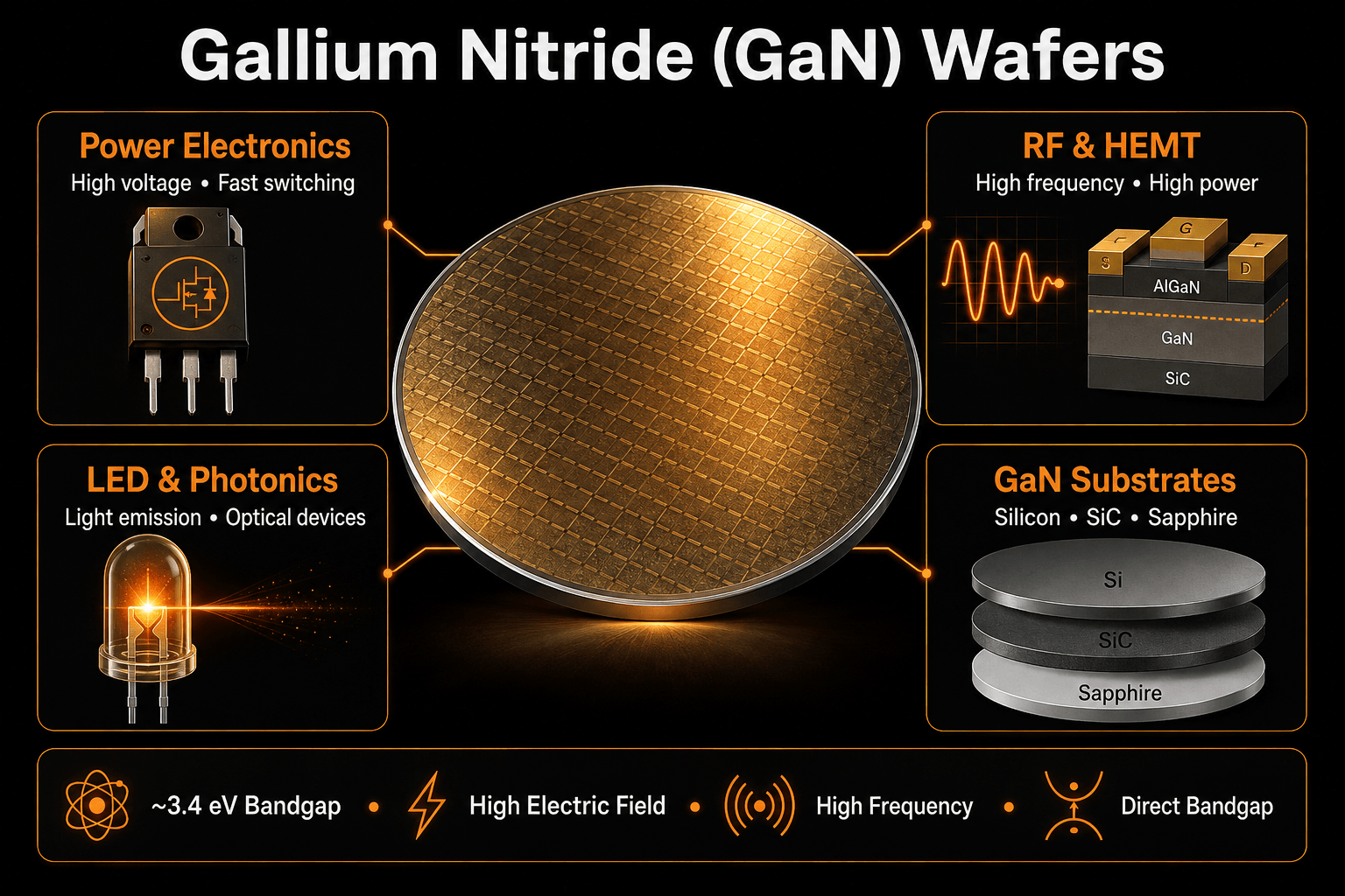
Gallium Nitride (GaN) wafers are wide-bandgap semiconductor materials used to develop electronic and optoelectronic devices that operate under demanding power, frequency, and temperature conditions. GaN has a direct bandgap of approximately 3.4 eV and is widely researched as an alternative to conventional silicon for specialized high-performance applications.
GaN can be used as a native substrate or grown epitaxially on materials such as silicon, silicon carbide (SiC), and sapphire.
GaN for Power Electronics
GaN's wide bandgap and high critical electric field make it attractive for research into efficient power semiconductor devices. Researchers investigate GaN technologies for faster switching, high power density, and reduced energy losses in advanced power-conversion systems.
- Power transistors
- High-voltage switching devices
- DC-DC converters
- Power supplies and adapters
- Electric vehicle power electronics
- Renewable-energy power conversion
GaN for RF and High-Frequency Devices
GaN heterostructures are also important for RF, microwave, and high-frequency semiconductor research. GaN-based devices can combine high power density with high-frequency operation, making the material valuable for communications and advanced electronic systems.
GaN HEMTs (High Electron Mobility Transistors) are particularly important for RF and power research because engineered heterostructures can create high-density, high-mobility electron channels.
GaN vs. Silicon for Semiconductor Research
Silicon remains essential for conventional semiconductor manufacturing, while GaN offers advantages for experiments involving higher electric fields, high-frequency operation, and optoelectronic devices.
| Property | GaN | Silicon |
|---|---|---|
| Bandgap | ~3.4 eV | ~1.12 eV |
| Bandgap Type | Direct | Indirect |
| Critical Electric Field | High | Lower |
| High-Frequency Applications | Excellent | Widely used, but more limited for extreme RF/power conditions |
| Optoelectronic Applications | LEDs, lasers, UV devices | More limited for light emission |
| Typical Research Focus | Power, RF, HEMT, LED, photonics | CMOS, ICs, MEMS, sensors |
GaN-on-Si, GaN-on-SiC or GaN-on-Sapphire?
The substrate underneath the GaN layer can significantly influence cost, thermal behavior, lattice mismatch, wafer availability, and the intended device application.
- GaN-on-Si – attractive for larger wafer formats and compatibility with silicon-based fabrication infrastructure.
- GaN-on-SiC – commonly investigated when excellent thermal management and high RF power performance are important.
- GaN-on-Sapphire – widely used for LEDs, optoelectronics, and material research.
Gallium Nitride Epitaxial Research
GaN epitaxy enables researchers to build carefully engineered semiconductor layer structures. Parameters such as layer thickness, doping, AlGaN composition, buffer layers, and interface quality can be adjusted to investigate specific device characteristics.
Epitaxial GaN wafers can support studies involving HEMT structures, power transistors, LEDs, photodetectors, material defects, surface processing, dielectric interfaces, and device reliability.
GaN Research Applications
- Wide-bandgap semiconductor research
- GaN HEMT fabrication
- High-voltage power devices
- RF and microwave electronics
- 5G and advanced communications research
- LED and laser diode development
- UV photonics and photodetectors
- Epitaxial growth studies
- Surface and interface characterization