
Premium Sapphire Wafers for Research & Manufacturing
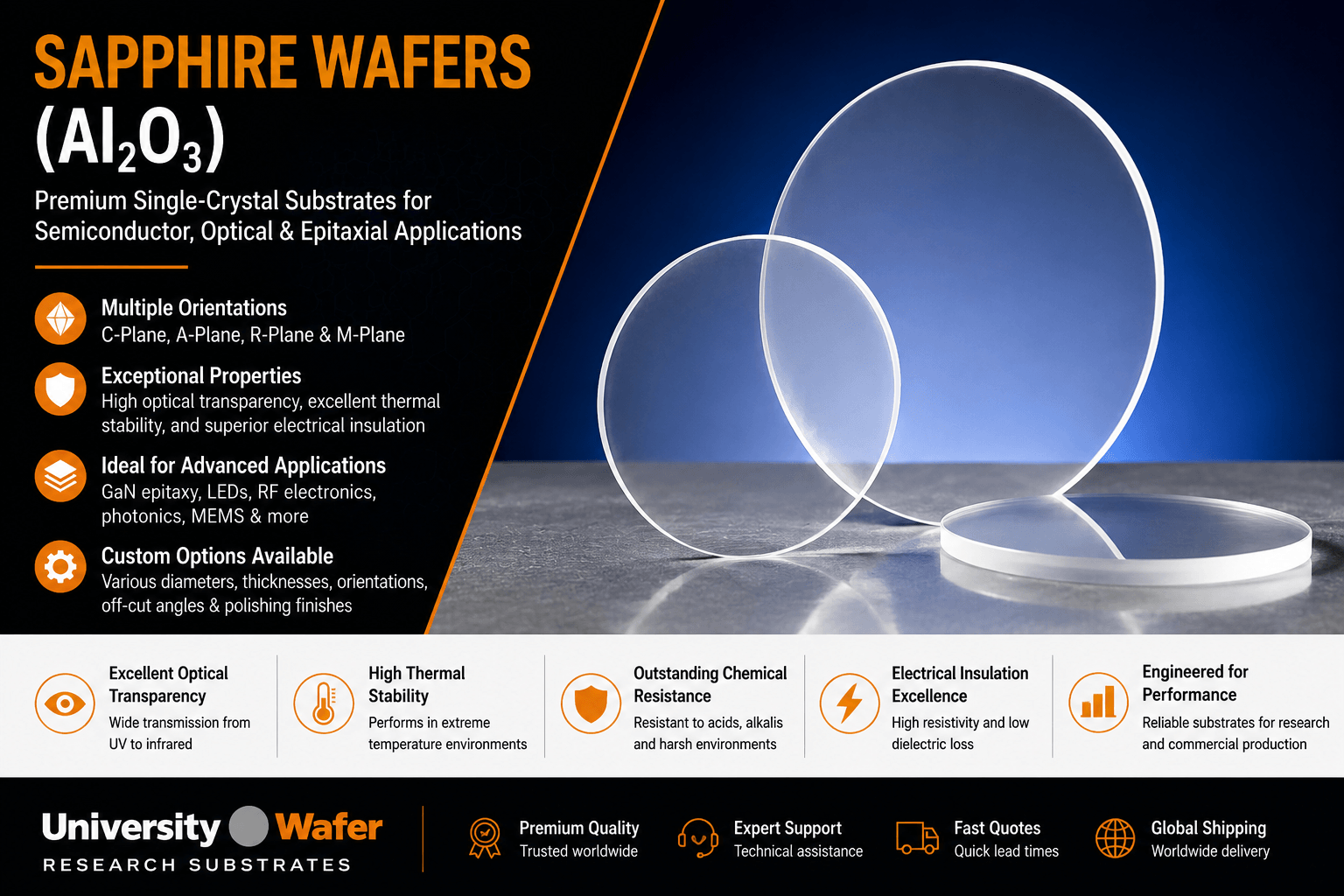
Sapphire wafers (Al₂O₃) are among the most widely used single-crystal substrates in the semiconductor and optoelectronics industries. Their outstanding mechanical strength, optical transparency, electrical insulation, and thermal stability make them the preferred substrate for GaN epitaxy, high-brightness LEDs, laser diodes, RF devices, MEMS, and advanced photonic systems. UniversityWafer supplies research-grade sapphire substrates to universities, national laboratories, and commercial manufacturers worldwide.
Our sapphire wafers are available in multiple crystallographic orientations, including C-plane, A-plane, R-plane, and M-plane, allowing researchers to select the ideal substrate for epitaxial growth, optical devices, microwave electronics, or specialized material science applications. We also offer custom diameters, thicknesses, off-cut angles, edge profiles, and polishing options to meet exact project specifications.
Applications of Sapphire Wafers
- Gallium nitride (GaN) epitaxy
- High-brightness LEDs and laser diodes
- RF and microwave electronics
- MEMS fabrication
- Optical windows and infrared optics
- Photonics and optoelectronics
- Sensors and biosensors
- Power electronics
- Quantum technology research
- University and government laboratory research
Custom Sapphire Wafer Options
UniversityWafer supplies custom sapphire substrates in a wide variety of wafer diameters, crystal orientations, thicknesses, polishing grades, and surface finishes. Whether you need prototype quantities for research or production volumes for commercial manufacturing, our technical team can recommend the ideal sapphire wafer for your application.
Get Your Sapphire Wafer Quote FAST! Or Buy Online and Start Researching Today!
Why Choose UniversityWafer?
For decades, UniversityWafer has been a trusted supplier of premium research substrates and semiconductor materials. Our sapphire wafers are manufactured to demanding quality standards and backed by expert technical support, fast quotations, competitive pricing, and worldwide shipping, helping researchers and manufacturers accelerate innovation across semiconductor, optical, and advanced materials applications.
What Are Sapphire Wafers (Al₂O₃)?
Sapphire wafers are single-crystal substrates manufactured from aluminum oxide (Al₂O₃). Known for their exceptional hardness, thermal stability, optical transparency, and electrical insulation, sapphire substrates are widely used in semiconductor fabrication, optoelectronics, photonics, RF electronics, MEMS, and scientific instrumentation. Their ability to withstand extreme temperatures and chemically aggressive environments makes them one of the industry's most reliable substrate materials.
Sapphire is commonly selected as the substrate for gallium nitride (GaN) epitaxy, enabling the production of high-brightness LEDs, laser diodes, power electronics, and RF devices. Different crystal orientations provide unique electrical, optical, and mechanical characteristics, allowing engineers to optimize substrate performance for specific applications.
Common Sapphire Crystal Orientations
| Orientation | Typical Applications |
|---|---|
| C-Plane (0001) | GaN epitaxy, LEDs, laser diodes, RF electronics, and power devices. |
| A-Plane (11-20) | Optical components, epitaxial growth, and anisotropic material research. |
| R-Plane (1-102) | Microwave devices, integrated optics, sensors, and specialty epitaxial films. |
| M-Plane (10-10) | Non-polar GaN growth, photonics, UV LEDs, and advanced optoelectronic devices. |
Key Material Properties
- Excellent optical transparency from UV through infrared wavelengths
- Exceptional hardness and scratch resistance (Mohs hardness of 9)
- High thermal conductivity and thermal stability
- Outstanding electrical insulation
- Excellent chemical and corrosion resistance
- Low dielectric loss for RF and microwave applications
- Compatible with high-temperature semiconductor processing
- Available in custom diameters, thicknesses, orientations, and surface finishes
Research & Industrial Applications
Researchers and manufacturers rely on sapphire wafers for high-brightness LEDs, GaN epitaxy, laser diodes, RF and microwave devices, MEMS, optical windows, infrared systems, biosensors, quantum technologies, microelectronics, and advanced photonic devices. Their outstanding combination of mechanical durability, thermal performance, and optical quality makes single-crystal sapphire one of the most versatile substrate materials available for both research laboratories and commercial semiconductor production.
UniversityWafer supplies premium research substrates, high-quality sapphire wafers (Al₂O₃), and custom single-crystal substrates manufactured to your exact diameter, orientation, thickness, and polishing requirements.