
Get Your GaN on SiC Wafer Quote FAST!
Gallium Nitride on Silicon Carbide (GaN on SiC) wafers are widely used for RF power amplifiers, microwave devices, radar systems, 5G infrastructure, satellite communications, HEMT fabrication, and advanced power electronics. Combining the high electron mobility of GaN with the excellent thermal conductivity of SiC creates a semiconductor platform capable of operating at higher frequencies, voltages, and temperatures than traditional silicon devices.
UniversityWafer supplies prime grade GaN on SiC substrates for semiconductor research, university laboratories, government programs, prototyping, and commercial production. Standard diameters range from 2-inch to 6-inch, with custom configurations available upon request.
Get Your GaN on SiC Quote FAST! Or, Buy Online and Start Researching Today!
Related Gallium Nitride Substrates
Custom GaN Wafer Capabilities
- Custom wafer diameters from 2" to 8"
- Single-side polished (SSP) and double-side polished (DSP) options
- Prime grade semiconductor quality
- Template thickness uniformity <10%
- Custom epitaxial layer thicknesses available
- N-type and semi-insulating substrate options
- Pricing based on wafer specifications and quantity requirements
Advantages of Gallium Nitride on Silicon Carbide (GaN on SiC) Wafers
Gallium Nitride on Silicon Carbide (GaN on SiC) is one of the most advanced wide-bandgap semiconductor platforms available for high-frequency, high-power, and high-temperature electronic devices. By combining the exceptional electron mobility of GaN with the superior thermal conductivity of silicon carbide (SiC), researchers and manufacturers can achieve significantly higher performance than conventional silicon-based technologies.
GaN-on-SiC substrates are widely used in RF amplifiers, microwave electronics, radar systems, 5G communications, satellite technology, defense applications, power electronics, HEMT devices, and next-generation semiconductor research. Their ability to operate at higher voltages, frequencies, and temperatures makes them ideal for demanding environments where efficiency and reliability are critical.
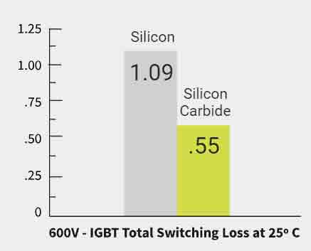
GaN on SiC devices can reduce switching losses by up to 50% compared to traditional silicon-based power devices, resulting in lower power consumption, faster switching speeds, reduced heat generation, and improved system efficiency.
Why Engineers Choose GaN on SiC
- Higher power density than conventional silicon devices
- Excellent thermal management due to the high thermal conductivity of SiC
- Fast switching speeds for RF and power applications
- Improved efficiency and reduced energy losses
- Outstanding performance in high-temperature environments
- Ideal for 5G, aerospace, defense, satellite, and microwave systems
- Suitable for high-electron-mobility transistor (HEMT) fabrication
Prime Grade GaN-on-SiC Wafer Specifications
UniversityWafer supplies prime grade GaN on Silicon Carbide wafers in multiple diameters and epitaxial thicknesses for semiconductor research, prototyping, and commercial production. Standard configurations include semi-insulating and n-type substrates with silicon or iron doping options.
GaN-on-Silicon Carbide (SiC) Wafer Series - Prime Grade |
|||||||
|---|---|---|---|---|---|---|---|
| Diameter | Orientation | Substrate Thickness | Surface Finish | GaN Template Thickness | Conduction Type | Dopant | Quantity |
| 2" | <0001> | 350 / 500 ±25 µm | DSP | 100–3000 nm | N-Type / Semi-Insulating | Si / Fe | ≤25 |
| 4" | <0001> | 350 / 500 ±25 µm | DSP | 100–3000 nm | N-Type / Semi-Insulating | Si / Fe | ≤25 |
| 6" | <0001> | 350 / 500 ±25 µm | DSP | 100–3000 nm | N-Type / Semi-Insulating | Si / Fe | ≤25 |
Custom GaN on SiC wafer specifications are available upon request, including different wafer diameters, epitaxial thicknesses, doping concentrations, and surface finishes. Contact UniversityWafer with your specifications and quantity requirements for a fast quotation.