
Thin-Film Stress Measurement Using Profilometry
Thin-film stress can strongly influence wafer bow, device reliability, coating adhesion, and overall process performance. One common method for evaluating residual film stress is to measure the curvature of a substrate before and after thin-film deposition using a surface profilometer.
Profilometer measurements provide a precise surface-height profile across the wafer. By comparing the substrate curvature before coating with the curvature after deposition, researchers can determine how much the deposited film has changed the wafer shape. This curvature change can then be used to estimate the film stress with the Stoney equation.
What Does a Profilometer Measure?
A profilometer measures surface topography by scanning across the substrate and recording changes in surface height. Depending on the instrument, the measurement may be performed with a physical stylus or by an optical, non-contact technique.
For thin-film stress measurements, the resulting surface profile can be analyzed to determine the wafer's radius of curvature. Accurate curvature measurements are especially useful when studying deposited films such as oxides, nitrides, metals, semiconductor layers, and other research coatings.
Using the Stoney Equation
The Stoney equation relates the change in substrate curvature to the biaxial stress present in a thin film. The calculation generally considers the substrate's elastic properties, substrate thickness, deposited film thickness, and the difference between the wafer curvature before and after deposition.
This method is most useful when the film is substantially thinner than the substrate and the substrate deformation remains within the assumptions of the Stoney model. Accurate film-thickness and wafer-curvature measurements are therefore important when calculating reliable stress values.
Why Thin-Film Stress Matters
Excessive tensile or compressive stress may produce wafer bow, cracking, delamination, surface defects, or dimensional changes during semiconductor processing. Monitoring stress allows researchers to compare deposition conditions and optimize processes before moving to more complex device fabrication.
Thin-film stress measurements are useful in research involving silicon wafers , dielectric coatings, MEMS structures, semiconductor processing, optical coatings, and experimental thin-film materials.
Substrate Quality Affects Measurement Accuracy
Reliable curvature measurements begin with high-quality substrates. Thickness uniformity, surface finish, wafer flatness, crystal orientation, and substrate mechanical properties can all affect the interpretation of thin-film stress measurements.
UniversityWafer supplies research-grade substrates in a wide range of materials, diameters, thicknesses, orientations, and surface finishes for thin-film deposition, profilometry, coating development, and materials characterization.
Get Your Thin-Film Stress Measurement Wafer Quote FAST! Or, buy online and start researching today!
Calculating Thin-Film Stress with the Stoney Equation
The Stoney equation is widely used to estimate the average biaxial stress in a thin film by measuring how deposition changes the curvature of a substrate. A profilometer can measure the wafer surface before and after deposition, allowing researchers to determine the curvature change associated with the deposited layer.
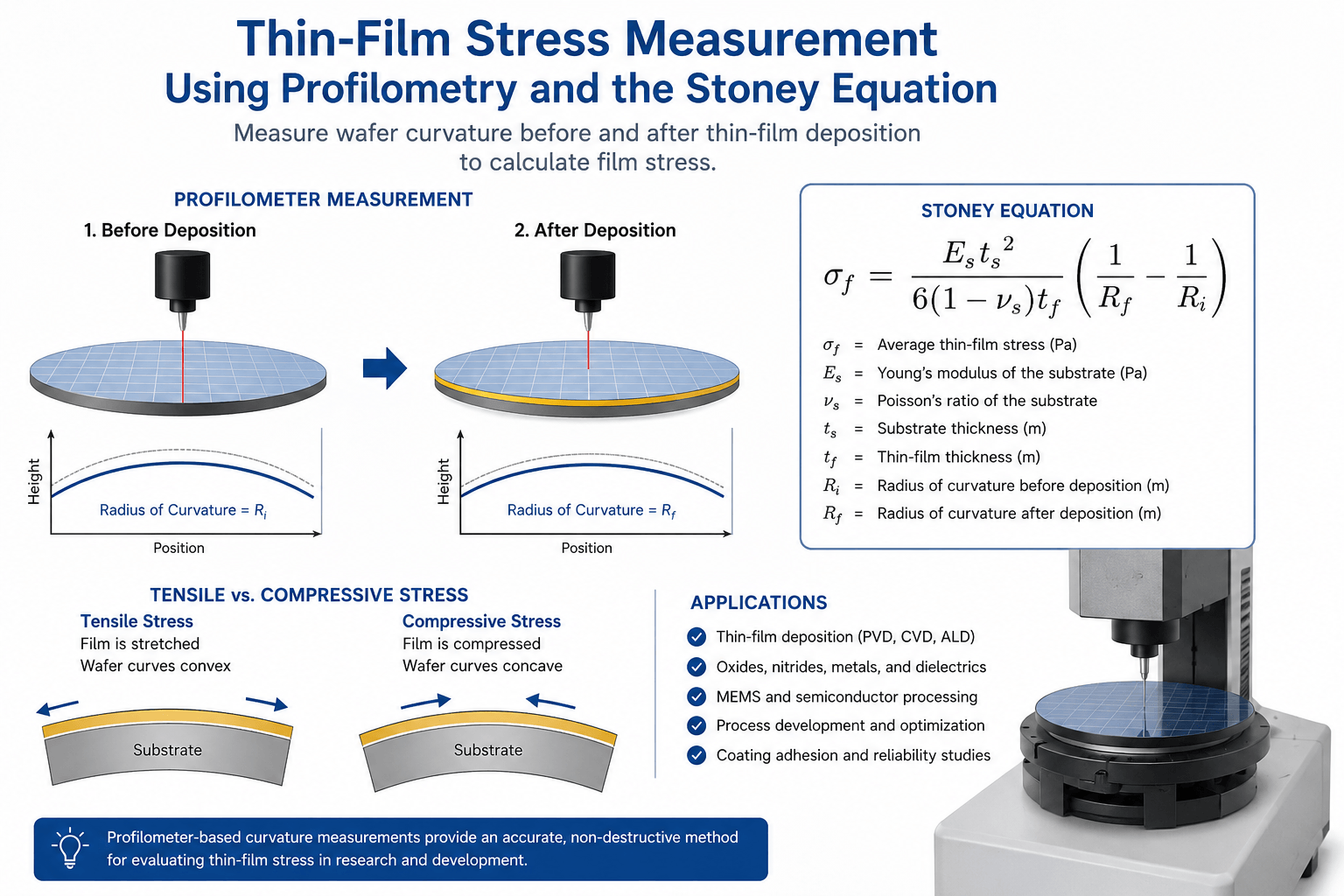
Stoney Equation
A commonly used form of the Stoney equation is:
σf = [Es ts2 / 6(1 − νs)tf] (1/Rf − 1/Ri)
Where:
- σf = average thin-film stress
- Es = Young's modulus of the substrate
- νs = Poisson's ratio of the substrate
- ts = substrate thickness
- tf = thin-film thickness
- Ri = substrate radius of curvature before deposition
- Rf = substrate radius of curvature after deposition
From Profilometer Data to Wafer Curvature
A profilometer records surface height as a function of position across the wafer. The measured profile can be fitted to determine the substrate curvature or radius of curvature. Measurements taken before and after film deposition provide the curvature values required for the Stoney equation.
Because thin-film stress calculations depend on relatively small changes in wafer curvature, consistent measurement locations and substrate positioning can help reduce measurement uncertainty.
Tensile vs. Compressive Thin-Film Stress
Deposited films may produce either tensile or compressive stress. Tensile stress tends to contract the film relative to the substrate, while compressive stress is associated with a film that tends to expand relative to the substrate.
The direction and magnitude of the resulting wafer curvature can therefore provide useful information about the mechanical state of the deposited film. Excessive residual stress can contribute to cracking, delamination, wafer bow, or changes in device performance.
Important Measurement Parameters
Accurate thin-film stress calculations depend on reliable measurements and material properties. Researchers should consider:
- Substrate thickness and thickness uniformity
- Thin-film thickness
- Initial wafer curvature before deposition
- Final wafer curvature after deposition
- Young's modulus of the substrate
- Poisson's ratio of the substrate
- Surface quality and wafer flatness
- Measurement position and scan length
When Is the Stoney Equation Appropriate?
The traditional Stoney equation is based on simplifying assumptions. It is most applicable when the deposited film is much thinner than the substrate and the film produces relatively small elastic deformation of the substrate.
Researchers working with relatively thick films, multilayer structures, highly anisotropic substrates, or large wafer deformations may need to consider additional mechanical models rather than relying exclusively on the basic Stoney equation.
Applications of Thin-Film Stress Measurements
Profilometer-based wafer curvature measurements can support process development and materials characterization across semiconductor and thin-film research. Common applications include:
- Physical vapor deposition (PVD) studies
- Chemical vapor deposition (CVD) research
- Thermal and deposited oxide films
- Silicon nitride thin films
- Metal and dielectric coatings
- MEMS fabrication
- Optical coating development
- Semiconductor process optimization
Using well-characterized wafers with known dimensions and material properties helps researchers establish a consistent substrate for comparing deposition conditions and evaluating thin-film stress.