
SOI Wafer Structure and Material Properties
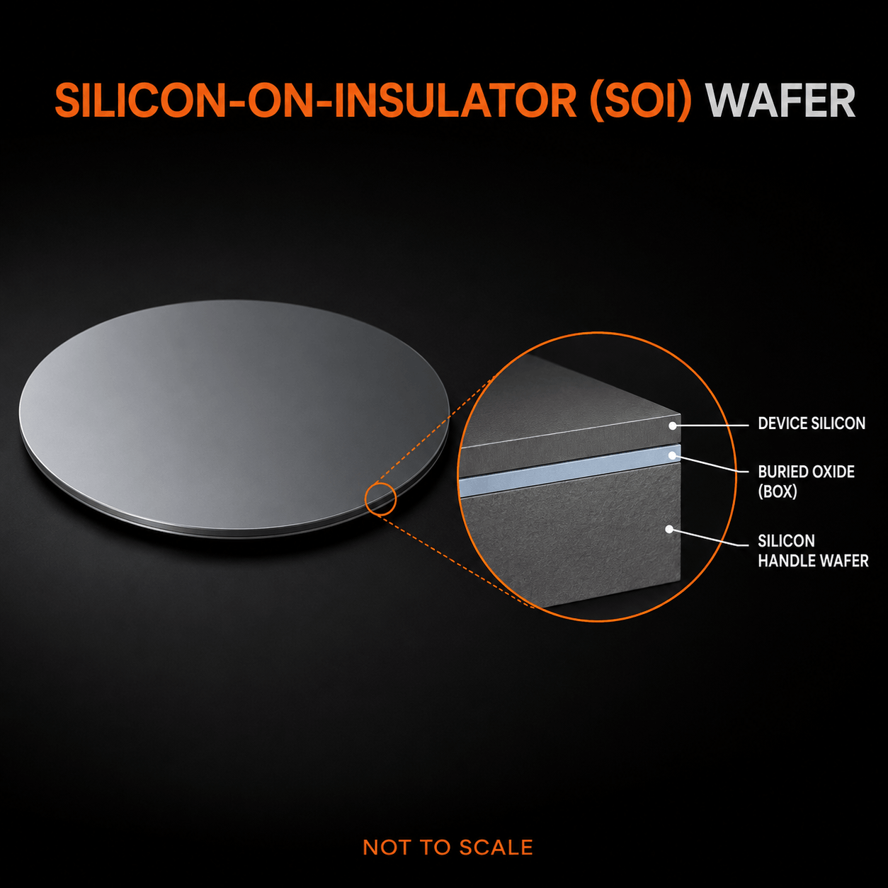
A silicon-on-insulator (SOI) wafer is an engineered substrate composed of a crystalline silicon device layer, an electrically insulating buried oxide (BOX) layer and a silicon handle wafer. Each layer can be selected to support specific fabrication, electrical and mechanical requirements.
Silicon Device Layer
The upper silicon layer is the active surface used to fabricate electronic, photonic and MEMS structures. Important specifications include device-layer thickness, crystal orientation, conductivity type, resistivity, thickness uniformity and surface finish.
Buried Oxide (BOX) Layer
The BOX layer electrically and thermally isolates the device layer from the silicon handle substrate. Its thickness influences capacitance, optical confinement, thermal behavior and the release of suspended MEMS structures.
Silicon Handle Wafer
The handle wafer provides mechanical support throughout processing and device fabrication. Handle-layer specifications may include wafer diameter, thickness, orientation, doping, resistivity, total thickness variation, bow and warp.
Common SOI Wafer Types
- Bonded SOI wafers
- SIMOX SOI wafers
- Thin-film SOI substrates
- Thick-device-layer SOI for MEMS
- High-resistivity SOI for RF applications
- SOI wafers for silicon photonics
- Custom device and BOX layer configurations
Bonded SOI and SIMOX
Bonded SOI is commonly produced by joining oxidized silicon wafers and thinning the upper silicon layer to the required specification. SIMOX wafers are manufactured using oxygen ion implantation followed by high-temperature annealing to form a buried oxide layer beneath the silicon surface.
Important Specifications
When selecting an SOI wafer, consider the wafer diameter, device-layer thickness, BOX thickness, handle thickness, crystal orientation, doping type, resistivity, surface finish and thickness uniformity. Particle levels, defect density, edge profile and thermal history may also be important for sensitive fabrication processes.
SOI Wafer Characterization
SOI wafers can be evaluated using ellipsometry, reflectometry, X-ray diffraction, four-point probe measurements, microscopy and surface-profiling techniques. Available documentation may include device and BOX thickness measurements, resistivity, total thickness variation, bow, warp and surface-quality data.
Need Custom Silicon-on-Insulator Wafers?
Provide UniversityWafer, Inc. with your required wafer diameter, device-layer thickness, BOX thickness, handle specifications, orientation, resistivity and quantity. Our team can help identify an SOI substrate suitable for your research and fabrication process.
Get Your SOI Wafer Quote FAST! Or, buy online and start researching today!
SOI Wafer Applications
Silicon-on-insulator wafers provide electrical isolation, controlled silicon device layers and reduced parasitic capacitance. These advantages make SOI substrates useful for fabricating MEMS, photonic, RF and advanced semiconductor devices.
MEMS and Sensor Fabrication
Thick-device-layer SOI wafers are widely used for MEMS because the device layer provides a controlled structural thickness while the buried oxide can serve as an etch-stop or sacrificial layer. Applications include accelerometers, pressure sensors, gyroscopes, resonators and microfluidic devices.
Silicon Photonics
SOI wafers are a common platform for silicon photonics. The refractive-index contrast between silicon and silicon dioxide helps confine light within the device layer, supporting waveguides, optical modulators, photodetectors, resonators and integrated photonic circuits.
RF and Microwave Electronics
High-resistivity SOI substrates can help reduce substrate losses, parasitic coupling and signal interference in RF devices. They are studied for switches, filters, amplifiers, antennas and wireless communication components.
CMOS and Low-Power Electronics
The insulating BOX layer separates active devices from the silicon handle wafer, reducing junction capacitance and electrical leakage. SOI technology supports research involving compact CMOS devices, low-power integrated circuits and radiation-tolerant electronics.
Power and High-Temperature Devices
SOI substrates can provide strong electrical isolation for devices designed to operate at elevated temperatures or voltages. They are used to investigate power-management circuits, automotive electronics and devices for demanding industrial environments.
Why Use SOI Instead of Bulk Silicon?
Compared with bulk silicon, SOI can offer improved device isolation, reduced parasitic capacitance and more precise control over the active silicon thickness. The best substrate depends on the required thermal behavior, electrical performance, device geometry and fabrication process.
Selecting an SOI Wafer
Specify the wafer diameter, device-layer thickness, buried oxide thickness, handle-wafer thickness, crystal orientation, conductivity type, resistivity, surface finish and quantity. For MEMS applications, also consider etch uniformity, layer-thickness tolerance, bow and total thickness variation.