
What Is a Field-Effect Transistor (FET)?
A Field-Effect Transistor (FET) is a semiconductor device that controls the flow of electrical current using an electric field. Unlike bipolar junction transistors (BJTs), FETs are voltage-controlled devices, requiring very little input current to regulate the conductivity of a semiconductor channel. Their low power consumption, high input impedance, and fast switching speeds make FETs the foundation of modern integrated circuits, processors, memory chips, and power electronics.
Nearly every smartphone, computer, electric vehicle, communication system, and consumer electronic device relies on billions of field-effect transistors fabricated on high-quality silicon wafers. Advances in transistor design continue to increase processing speed while reducing power consumption and device size.
Major Types of Field-Effect Transistors
- MOSFET (Metal-Oxide-Semiconductor FET) — The most widely used transistor in digital and analog integrated circuits.
- JFET (Junction Field-Effect Transistor) — Controls current through a reverse-biased p-n junction.
- FinFET — A three-dimensional transistor architecture used in advanced semiconductor nodes for improved performance and reduced leakage.
- Thin-Film Transistor (TFT) — Commonly used in LCD displays, OLED displays, and flexible electronics.
Semiconductor Materials Used for FETs
Although silicon remains the dominant semiconductor material, modern FET research also investigates compound semiconductors and wide-bandgap materials to achieve higher switching speeds, improved efficiency, and better high-temperature performance. UniversityWafer supplies substrates including Silicon, III-V Semiconductor Wafers, Silicon Carbide (SiC), and Gallium Nitride (GaN) for advanced transistor research.
Get Your Semiconductor Wafer Quote FAST! Or Buy Online and Start Researching Today!
How Does a Field-Effect Transistor Work?
A Field-Effect Transistor (FET) controls the flow of current through a semiconductor channel using an electric field generated by the gate terminal. Unlike bipolar transistors that require current to operate, FETs are voltage-controlled devices. Applying a voltage to the gate changes the conductivity of the channel between the source and drain, allowing precise control of electrical current with minimal power consumption.
This operating principle makes FETs ideal for integrated circuits, high-speed processors, analog electronics, RF communication systems, and low-power portable devices. Modern semiconductor manufacturing depends on extremely clean, defect-free silicon wafers to fabricate billions of transistors on a single chip.
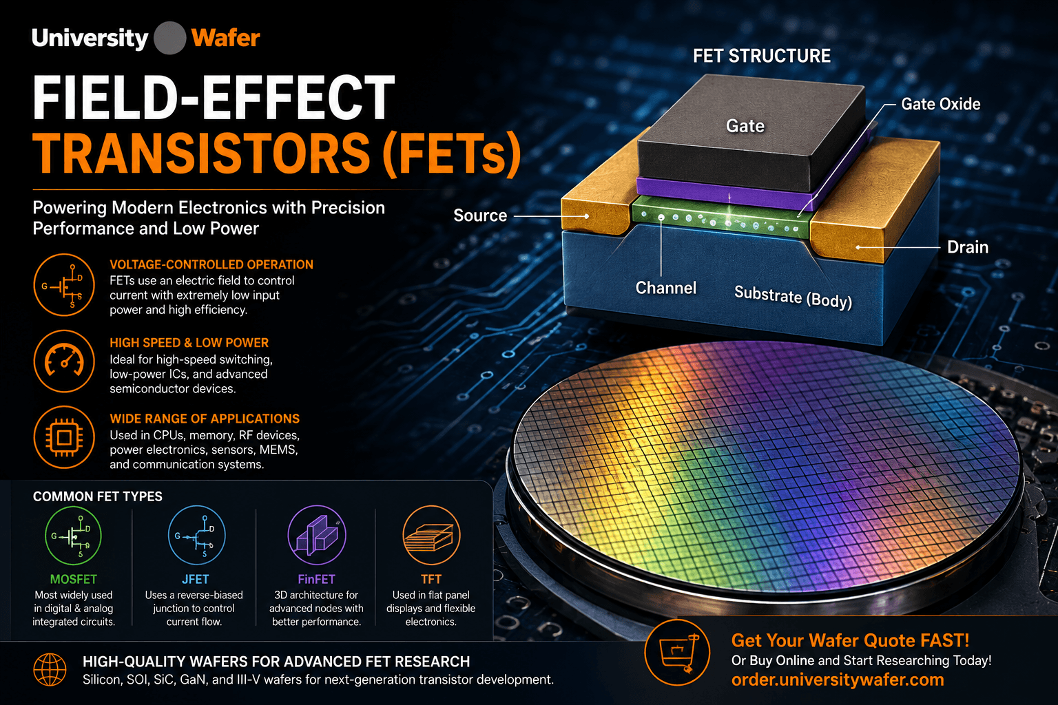
Main Components of a FET
- Gate – Controls the electric field that regulates current flow.
- Source – The terminal where charge carriers enter the transistor.
- Drain – The terminal where charge carriers exit the device.
- Channel – The conductive path between the source and drain.
- Substrate (Body) – The semiconductor material supporting the transistor structure.
- Gate Oxide – An insulating dielectric layer that separates the gate from the channel in MOSFET devices.
Applications of Field-Effect Transistors
FETs are used in virtually every area of modern electronics because of their fast switching speeds, low power requirements, and high reliability. Common applications include:
- Microprocessors and CPUs
- Memory devices (DRAM, SRAM, Flash)
- Artificial intelligence (AI) processors
- Power management circuits
- RF and wireless communication systems
- Automotive electronics and electric vehicles
- Sensors and MEMS devices
- Medical electronics
- Consumer electronics and mobile devices
Semiconductor Wafers for FET Research
The performance of field-effect transistors depends on the quality of the underlying semiconductor substrate. UniversityWafer supplies research-grade silicon wafers, SOI wafers, Silicon Carbide (SiC), Gallium Nitride (GaN), and III-V semiconductor substrates used in advanced transistor development, power electronics, photonics, RF devices, and university research.