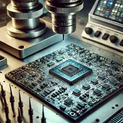
Microelectronics: Wafers, Films & Fabrication Materials
UniversityWafer, Inc. supplies the substrates and thin films that power today’s microelectronics research and industrial manufacturing. Our wafers enable lithography, etching, deposition, and packaging processes used to build micro- and nano-scale devices for computing, communications, photonics, and energy systems.
Get Wafers and Films for Microelectronics Research
Find Silicon, SOI, SiC, GaN, and GaAs wafers along with oxide, nitride, and polyimide coatings for every stage of your device development — from lithography to packaging.
Get Your Wafer Quote FAST! Or, Buy Online and Start Researching Today!
What We Offer
- Silicon wafers: 100–300 mm prime, DSP, SSP, high resistivity, custom doping.
- SOI wafers: Device/BOX/Handle configurations for MEMS or CMOS research.
- Compound semiconductors: GaN, SiC, GaAs, and InP for power and RF devices.
- Dielectrics & coatings: Oxide, Nitride, and Polyimide films for isolation and passivation.
- Custom fabrication: Film thickness control, orientation, and double-side polish on request.
Microelectronics in Research & Industry
Microelectronics forms the foundation for integrated circuits, MEMS sensors, power devices, and RF communication systems. Research groups and companies use our wafers to prototype everything from quantum chips to flexible electronics.
- Universities use Si and SOI wafers for cleanroom teaching labs.
- MEMS teams etch anisotropic silicon cavities for pressure sensors.
- Power electronics firms develop GaN and SiC devices for EV and grid applications.
- Photonics startups fabricate silicon photonics and LiNbO₃ modulators.
Quick Spec Template (Copy/Paste)
- Substrate: Si(100) / Si(111) / GaN / SiC
- Diameter: 100 mm / 150 mm / 200 mm / 300 mm
- Thickness: ___ µm | TTV ≤ ___ µm | Bow ≤ ___ µm
- Films: Thermal SiO₂ ___ µm | Si₃N₄ ___ nm | Polyimide ___ µm
- Doping: n-type / p-type (Phosphorus, Boron, or Arsenic)
- Surface: DSP / SSP / Oxide / Nitride
- Resistivity: ___ Ω·cm (specify range)
Why Choose UniversityWafer?
- Extensive in-stock inventory for rapid turnaround.
- Custom wafer fabrication and film growth.
- Small-quantity research orders and large-volume production support.
- Experienced team supporting universities and global R&D labs.
What Is Microelectronics?
Microelectronics is the science and engineering of manufacturing miniature electronic devices at the micrometer and nanometer scale. It merges materials science, physics, and semiconductor processing to fabricate integrated circuits (ICs), sensors, actuators, and power devices on precisely engineered wafers. Every smartphone, automobile, and satellite relies on microelectronics for data processing, sensing, and communication.
Modern microelectronic fabrication involves more than 1,000 process steps from raw silicon crystal growth to final chip packaging. Critical stages include wafer slicing and polishing, thin-film deposition, pattern transfer via photolithography, etching, doping, and metallization. Advances such as 5 nm node manufacturing and 3D stacking now push beyond Moore’s Law into heterogeneous and quantum domains.
Core Materials & Substrate Platforms
Microelectronics relies on crystalline substrates that act as both structural and electrical platforms:
- Silicon (Si): The universal semiconductor; supports CMOS logic, analog, MEMS, and power ICs. Available in diameters from 25 mm to 300 mm.
- Silicon-on-Insulator (SOI): Enables low-leakage devices, RF isolation, and precision MEMS cavities. Learn more at SOI wafers.
- Compound semiconductors: SiC and GaN deliver wide-bandgap performance for high voltage and frequency; GaAs and sapphire support photonics, LEDs, and RF circuits.
Thin Films & Dielectric Engineering
Device performance depends heavily on controlled thin-film stacks. At each layer, uniformity, stress, and interface quality are critical:
- Thermal oxide (SiO₂): Key dielectric for MOSFET gates and isolation. Typical growth rates: 10 nm/min at 1000 °C. See Thermal Oxide Wafers.
- Silicon nitride (Si₃N₄): Excellent diffusion barrier and passivation; deposited by LPCVD or PECVD. See SiN Wafers.
- Polyimide (PI): Used as a flexible dielectric for redistribution layers (RDL), stress relief, and packaging. See Polyimide Films.
- Metallization layers: Cu, Al, W, or TiN are used for interconnects, diffusion barriers, and contact pads.
Patterning, Etching & Deposition Techniques
Each integrated device is built through layer-by-layer patterning and selective removal or addition of materials:
- Photolithography: UV exposure through masks defines circuit geometries from tens of microns to below 100 nm. Current leading-edge fabs employ EUV (13.5 nm wavelength) for sub-7 nm resolution.
- Etching: Wet etches such as KOH/TMAH anisotropic etching form precision V-grooves, while RIE and DRIE provide vertical profiles up to 100:1 aspect ratio.
- Deposition: Physical Vapor Deposition (PVD), Chemical Vapor Deposition (CVD), and Atomic Layer Deposition (ALD) create conformal metal, dielectric, or semiconductor films down to sub-nanometer control.

Packaging, Interconnects & Heterogeneous Integration
Microelectronic packaging has evolved from simple wire-bonded dies to wafer-level and 3D integrated assemblies. Recent developments include:
- Fan-out wafer-level packaging (FOWLP): Redistributes I/O pads using polyimide or epoxy dielectrics and Cu RDLs for ultra-thin system-in-package (SiP) designs.
- Through-silicon vias (TSVs): Deep-etched holes filled with Cu to create vertical interconnects, enabling 3D integration of memory, logic, and sensors.
- Chiplet architectures: Multiple specialized dies connected through high-density interposers, improving performance and yield over monolithic SoCs.
Emerging Trends & Research Directions
The field continues to expand into new frontiers:
- Wide-bandgap electronics: GaN and SiC enable higher power efficiency and switching frequencies for EVs and power grids.
- Flexible and bio-integrated microelectronics: Thin polyimide substrates allow wearable and implantable sensor systems.
- Quantum and neuromorphic chips: Superconducting junctions and memristor arrays simulate neural networks at nanoscale power levels.
- Heterogeneous integration: Combines optical, mechanical, and electronic functions on a single wafer platform.
Research & Development Use-Cases
University and industrial researchers routinely request:
- 100–150 mm Si(100) wafers with thermal oxide/nitride stacks for CMOS and MEMS prototyping.
- SOI wafers with 1 µm device layer / 100 nm BOX for MEMS cavity formation.
- GaN-on-Si 200 mm wafers for RF and power transistor development.
- Quartz and glass wafers with polyimide coatings for optical sensors and flexible devices.
