
What Is Silicon Wafer Reclaiming?
Silicon wafer reclaiming is the process of reconditioning suitable used silicon wafers so they can be reused for applications such as semiconductor process monitoring, equipment qualification, deposition trials, and research. Depending on the wafer's previous processing and condition, reclaiming can involve film removal, surface reconditioning or polishing, cleaning, inspection, and dimensional verification.
Reclaiming is particularly useful for test and monitor wafers that do not need to serve as the starting substrate for finished integrated circuits. By extending the useful life of suitable wafers, reclaiming can reduce the consumption of new silicon substrates while providing economical wafers for many non-device applications.
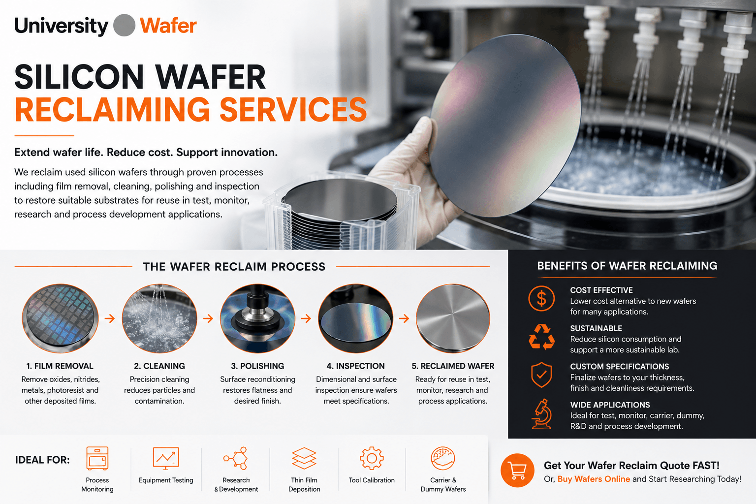
How the Silicon Wafer Reclaim Process Works
The exact wafer reclaim process depends on the materials present on the wafer, its surface condition, its processing history, and the specifications required after reclaim. A typical process may include several of the following stages:
- Incoming inspection: Wafers are evaluated for physical condition, dimensions, surface films, contamination, edge damage, and other characteristics relevant to reclaimability.
- Film removal: Deposited or grown materials are removed using chemistry and processes selected for the particular film stack.
- Surface reconditioning: When required, controlled polishing removes surface damage, residual material, or a thin portion of the silicon substrate and restores an appropriate surface finish.
- Cleaning: The wafer is cleaned to reduce particles, organic residues, metallic contamination, and other unwanted surface contaminants.
- Inspection and metrology: Reclaimed wafers can be evaluated for parameters such as thickness, TTV, bow, warp, surface condition, particles, and other application-specific requirements.
Removing Films from Used Silicon Wafers
Used wafers may contain materials deposited during previous semiconductor processing. Depending on the application, these can include silicon dioxide (SiO2), silicon nitride (Si3N4), photoresist, polysilicon, metals, or multilayer film stacks.
Film-removal chemistry must be selected according to the materials present. Different films require different stripping or etching processes, and inappropriate chemistry or excessive processing can attack the underlying silicon, increase surface roughness, produce defects, or introduce contamination.
For this reason, information about the wafer's previous processing and film composition can be valuable when determining an appropriate reclaim sequence.
Wafer Polishing and Surface Reconditioning
After unwanted layers have been removed, some wafers require surface polishing to restore the surface condition needed for reuse. Chemical-mechanical polishing (CMP) combines chemical interactions with controlled mechanical action to remove material and produce a smoother, more planar surface.
Learn more about chemical mechanical polishing (CMP) and its role in semiconductor wafer planarization and surface preparation.
Polishing must be carefully controlled because it removes silicon from the substrate. Excessive material removal can change wafer thickness, thickness uniformity, geometry, and ultimately the wafer's compatibility with processing equipment.
Cleaning Reclaimed Silicon Wafers
Cleaning is an important part of wafer reclamation because stripping and polishing alone do not guarantee a sufficiently clean surface. Depending on the required application, cleaning processes may be designed to reduce particles, organic contamination, metallic residues, polishing residues, and other surface contaminants.
Cleaning chemistry should be selected according to the contamination present and the required final surface condition. Semiconductor cleaning processes may use combinations of aqueous chemistry, rinsing, mechanical assistance, and controlled drying.
Researchers can also explore ultrasonic wafer cleaning for more information about particle and contaminant removal from substrate surfaces.
Reclaimed Wafers for Test and Monitor Applications
Reclaimed silicon wafers are particularly useful as test, monitor, or process-development substrates. Semiconductor manufacturing and research facilities use monitor wafers to evaluate processes without consuming a new prime wafer for every experiment.
Depending on the required specifications, reclaimed wafers can be useful for:
- Thin-film deposition monitoring
- Film-thickness measurements
- Etch-rate characterization
- Oxidation process monitoring
- Particle and contamination monitoring
- CMP process development
- Equipment qualification and testing
- Process development and laboratory research
The suitability of a reclaimed wafer for any of these applications depends on its final surface, dimensional, cleanliness, and electrical requirements.
Reclaimed Wafers vs. New Prime Wafers
A reclaimed wafer should not automatically be considered equivalent to a new prime wafer. Prime wafers are manufactured to specifications intended for demanding semiconductor fabrication, while reclaimed wafers have undergone previous processing followed by one or more reconditioning steps.
Reclaiming may remove a portion of the original silicon and can alter wafer thickness or other characteristics. For this reason, reclaimed substrates are commonly used where their verified final specifications are sufficient, rather than assuming they are interchangeable with new device-grade substrates.
Can Every Silicon Wafer Be Reclaimed?
Not every used wafer is a suitable candidate for reclamation. Reclaimability depends on factors such as remaining wafer thickness, edge condition, cracks, chips, surface damage, contamination history, deposited materials, implanted or diffused regions, and the specifications required after processing.
Wafers with severe mechanical damage or insufficient remaining thickness may not be practical to reclaim. Certain contamination or process histories can also require specialized handling or make a wafer unsuitable for a particular future application.
An incoming inspection is therefore important before determining whether a used wafer can be successfully reconditioned.
How Many Times Can a Silicon Wafer Be Reclaimed?
There is no universal number of times that a silicon wafer can be reclaimed. The usable reclaim life depends on the starting thickness, amount of silicon removed during each cycle, accumulated surface or edge damage, wafer geometry, contamination history, and the minimum specifications required for its next application.
Because polishing and some surface-reconditioning processes remove substrate material, wafer thickness generally decreases over repeated reclaim cycles. Eventually, a wafer may no longer meet the dimensional or mechanical requirements of the equipment or process in which it is intended to be used.
Benefits of Silicon Wafer Reuse
Reclaiming suitable wafers can reduce the number of new substrates consumed by applications that do not require new prime-grade material. This can provide both economic and material-efficiency benefits, particularly in environments where large numbers of wafers are used for process monitoring and equipment testing.
Reuse should still be based on technical requirements. The objective is not simply to reuse every wafer, but to determine whether a reclaimed substrate meets the specifications needed for its intended next process.
Specify Your Silicon Wafer Reclaim Requirements
When requesting silicon wafer reclaiming services, useful information can include wafer diameter, starting thickness, conductivity type, resistivity, surface finish, existing film stack, previous processing, contamination concerns, quantity, and the required final specifications.
Clearly defining the intended reuse application also helps determine which surface, cleanliness, dimensional, and inspection requirements are important after reclaim.
Get Your Silicon Wafer Reclaiming Quote FAST!
Or, Buy Wafers Online and Start Researching Today!
Qualifying Silicon Wafers for Reclaim
Before a used wafer is reclaimed, it should be evaluated to determine whether its physical condition and process history are compatible with the required final specification. Silicon wafer reclaiming is most useful when the substrate remains mechanically sound and can tolerate the material removal and cleaning required during reconditioning.
Important considerations can include wafer diameter, remaining thickness, TTV, bow, warp, edge condition, surface damage, existing films, contamination history, and previous processing. Wafers with severe cracking, excessive edge damage, insufficient thickness, or problematic contamination may not be suitable for economical reclamation.
Reclaim Specifications Depend on the Final Application
A reclaimed wafer does not need the same specification for every application. A substrate intended as a dummy wafer for equipment testing may tolerate characteristics that would be unacceptable for precision lithography or demanding thin-film research.
For this reason, reclaimed silicon wafer specifications should be based on the next intended process. Depending on the application, relevant requirements can include:
- Final wafer thickness and thickness tolerance
- Total thickness variation (TTV)
- Bow and warp
- Surface finish and roughness
- Particle and contamination limits
- Edge condition
- Front-side or double-side surface requirements
- Electrical properties when relevant to the application
Reclaimed Wafers for Process Monitoring
Reclaimed silicon wafers can be useful for semiconductor process monitoring when a new prime-grade substrate is unnecessary. Monitor wafers provide a controlled surface on which researchers and process engineers can evaluate equipment and fabrication processes.
Depending on their final specifications, reclaimed wafers may be used for deposition monitoring, etch testing, oxidation studies, CMP development, particle monitoring, coating trials, equipment qualification, and process characterization.
Researchers who need economical substrates can also explore reclaimed silicon wafers for carrier and dummy applications .
Carrier and Dummy Silicon Wafers
Reclaimed wafers are often suitable for carrier, dummy, and sacrificial wafer applications. In these roles, the silicon substrate may support another sample, occupy a process position, protect equipment conditions, or provide a surface for preliminary process testing.
Carrier-wafer requirements depend on the process. Diameter, thickness, flatness, thermal behavior, surface condition, and compatibility with the processing environment can all matter. A reclaimed wafer should therefore still be selected according to its intended use rather than simply because it is less expensive than a new wafer.
Reclaiming Wafers After Thin-Film Deposition
Silicon wafers used for thin-film deposition experiments may be candidates for reclaim if the deposited materials can be removed without unacceptable damage to the substrate. The appropriate stripping process depends on the chemical and physical properties of the film stack.
Films such as oxides, nitrides, photoresists, polysilicon, and metals require different removal approaches. Multilayer structures may require several sequential stripping processes.
Film removal should therefore be based on the known composition of the stack. A stripping chemistry that selectively removes one material may attack another layer or the underlying silicon under different conditions.
CMP and Wafer Reclaiming
Chemical mechanical polishing (CMP) can be used as part of wafer surface reconditioning when controlled material removal and polishing are required. CMP combines chemical and mechanical mechanisms to remove material and modify surface topography.
The amount of silicon removed during polishing should be controlled because it affects the wafer's final thickness and geometry. Repeated polishing can eventually make a wafer too thin or otherwise unsuitable for its intended equipment or process.
Reclaiming vs. Wafer Backgrinding
Wafer reclaiming and wafer backgrinding are not the same process. Reclaiming is intended to recondition a previously processed wafer for reuse, whereas backgrinding is primarily used to reduce substrate thickness by mechanically removing material from the backside.
Silicon wafer backgrinding is commonly used when a specific thinner substrate or device-wafer thickness is required. Grinding can leave subsurface damage and grinding marks, so additional processing or polishing may be required when a smoother surface is necessary.
A reclaim sequence may involve polishing or other surface reconditioning, but reclaiming should not be described simply as wafer thinning.
Surface Cleaning After Wafer Reclaim
Cleaning after film removal and polishing is important because particles, polishing residues, organic material, metals, and other contaminants can remain on the wafer surface. The required cleaning sequence depends on the contaminants present and the cleanliness needed for the next process.
Traditional silicon cleaning approaches can include RCA wafer cleaning , solvent cleaning, oxide-removal steps, and particle-removal techniques. However, no single cleaning sequence is appropriate for every reclaimed wafer.
Cleaning chemistry must be compatible with the substrate and any materials that remain on it. Surface requirements for subsequent epitaxy, deposition, bonding, or device processing can be considerably more demanding than those for a dummy or equipment-test wafer.
Contamination History Matters
A wafer's previous process history can influence whether it is appropriate for reuse. Semiconductor processes can expose wafers to metals, dopants, photoresists, polymers, etchants, deposition precursors, and other materials.
Some contaminants can be difficult to remove completely or may be unacceptable in a subsequent process because of cross-contamination concerns. For contamination-sensitive applications, it is therefore useful to provide as much information as possible about the wafer's previous use.
A visually clean surface should not automatically be assumed to satisfy a particular chemical or contamination specification.
Dimensional Changes During Reclaim
Surface reconditioning can remove a small amount of silicon, meaning that a reclaimed wafer may be thinner than it was before processing. Repeated reclaim cycles can progressively reduce wafer thickness.
Geometry should also be considered because thickness, TTV, bow, and warp can affect wafer handling, chucking, lithography, deposition, measurement, and other processes. The final wafer should be evaluated against the dimensional requirements of its intended application.
This is one reason there is no universal maximum number of times a silicon wafer can be reclaimed.
Prime, Test and Reclaimed Silicon Wafers
Different wafer grades serve different purposes. Prime silicon wafers are appropriate when tightly controlled surface, dimensional, crystal, or electrical characteristics are required for demanding device fabrication. Test wafers can provide a lower-cost option for process development and monitoring.
Reclaimed wafers provide another option when the required final specifications can be achieved through reconditioning. They are particularly attractive for applications where consuming a new prime wafer would provide little technical benefit.
The choice should be based on the actual process requirements rather than assuming that prime, test, and reclaimed wafers are interchangeable.
Reclaiming Different Silicon Wafer Sizes
Reclaim processes can be applied to multiple silicon wafer diameters when compatible handling, stripping, polishing, cleaning, and metrology equipment are available. The practical process requirements change with wafer diameter, thickness, and condition.
Larger wafers can place tighter demands on uniform material removal and geometry control because process nonuniformity extends across a larger substrate area. Final dimensional requirements should therefore be specified for the particular wafer size being reclaimed.
For larger-diameter research and equipment applications, explore 300 mm silicon wafers and available substrate specifications.
When Should You Use a Reclaimed Wafer?
A reclaimed wafer is a strong candidate when the application requires a silicon substrate but does not require a new prime wafer. Common examples include process development, equipment testing, tool calibration, carrier-wafer use, deposition experiments, etch trials, cleaning studies, training, and other sacrificial processes.
A new prime wafer may be more appropriate when the experiment depends on tightly controlled crystal quality, surface condition, electrical properties, contamination limits, or other specifications that cannot be reliably achieved by the available reclaim process.
Information to Include With a Wafer Reclaim Request
Providing detailed information helps determine whether a batch of wafers is suitable for reclamation and which processing steps may be required. Useful information includes:
- Wafer material and diameter
- Starting or current thickness
- Quantity
- Existing films or coatings
- Previous processing or contamination history
- Surface condition and visible damage
- Required final thickness and geometry
- Required surface finish
- Cleanliness requirements
- Intended reuse application
The final specification should be based on the requirements of the next process so that unnecessary polishing, metrology, or other processing is avoided while still producing a wafer suitable for reuse.
Related Silicon Wafer Reclaiming & Processing Resources
- Reclaimed Silicon Wafers – Explore reclaimed silicon substrates for process development, equipment testing, carrier wafers, dummy wafers, and research.
- Chemical Mechanical Polishing (CMP) – Learn how controlled chemical and mechanical material removal is used for wafer planarization and surface preparation.
- Silicon Wafer Backgrinding – Explore backside grinding for reducing silicon wafer thickness and preparing substrates for applications requiring thinner wafers.
- Ultrasonic Wafer Cleaning – Learn about ultrasonic cleaning techniques for removing particles and contaminants from wafer and substrate surfaces.
- RCA Silicon Wafer Cleaning – Learn about established wet-chemical cleaning sequences used to remove selected organic, particulate, and metallic contamination from silicon surfaces.
- Silicon Wafer Surface Roughness – Understand how surface roughness is characterized and why it matters for polished and reconditioned silicon substrates.
- Atomic Force Microscopy (AFM) – Explore nanoscale surface topography and roughness characterization for silicon wafers and thin films.
- Silicon Wafer Total Thickness Variation (TTV) – Learn why thickness uniformity is an important geometric specification for reclaimed and precision-processed wafers.
- 300 mm Silicon Wafers – Explore large-diameter silicon substrates for semiconductor processing, equipment testing, monitoring, and research.
- Semiconductor Wafers – Learn about semiconductor substrate materials, wafer grades, specifications, and applications in research and fabrication.
- Semiconductor Wafer Quality – Explore wafer surface, dimensional, electrical, crystallographic, inspection, and quality considerations.
- Silicon Wafers – Browse silicon substrates with different diameters, orientations, doping types, resistivities, thicknesses, and surface finishes.