
What Defines Semiconductor Wafer Quality?
Semiconductor wafer quality is determined by whether a substrate meets the material, dimensional, electrical, crystallographic, and surface requirements of its intended application. There is no single specification that defines a high-quality wafer for every process. A wafer suitable for routine testing may have very different requirements from one intended for epitaxy, photolithography, wafer bonding, MEMS, photonics, or advanced device fabrication.
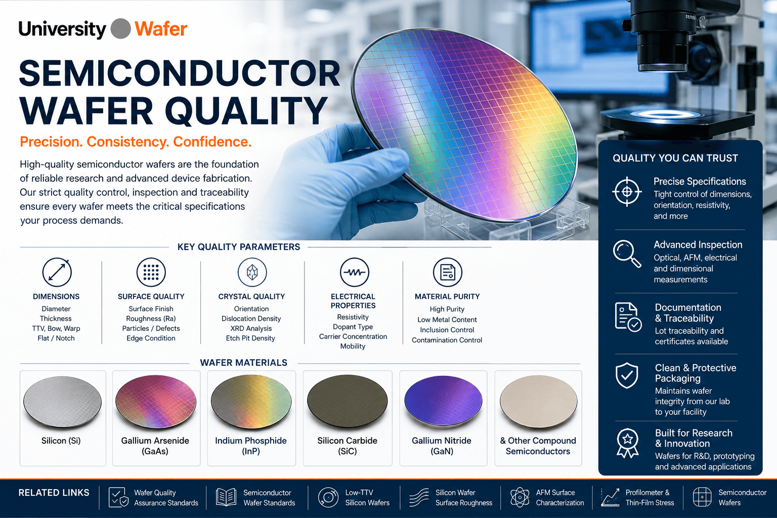
Important parameters can include material purity, crystal orientation, dopant type, resistivity, diameter, thickness, total thickness variation (TTV), bow, warp, surface finish, surface roughness, and defect levels. Understanding these specifications helps researchers choose substrates that are compatible with their fabrication and characterization processes.
Wafer Surface Quality and Cleanliness
Surface condition is especially important when a wafer will undergo thin-film deposition, lithography, epitaxial growth, bonding, or nanoscale characterization. Particles, scratches, residues, pits, excessive roughness, and other surface defects can interfere with subsequent processing or measurements.
Silicon wafer surface roughness describes the microscopic variation in surface height over a specified measurement area. Techniques such as atomic force microscopy (AFM) and optical methods can be used to characterize surface topography and roughness, depending on the required lateral and vertical measurement scales.
Surface-finish requirements should always be matched to the application. Single-side polished wafers can be appropriate for many front-side processes, while double-side polished substrates are often selected when both surfaces, wafer symmetry, optical transmission, bonding, or double-sided processing are important.
Thickness, TTV, Bow and Warp
Wafer geometry influences how a substrate interacts with processing and measurement equipment. In addition to nominal thickness, important dimensional specifications can include total thickness variation (TTV), bow, warp, diameter tolerance, and edge geometry.
TTV describes the difference between the maximum and minimum wafer thickness under a defined measurement condition. Bow and warp describe different aspects of wafer shape and deviation from an ideal reference plane. These parameters can become especially important for photolithography, wafer bonding, MEMS processing, thin-film deposition, and precision handling.
The acceptable values are application-specific. A research experiment that does not depend strongly on wafer flatness may tolerate wider dimensional limits than a process involving precision alignment or bonding.
Crystal Orientation and Wafer Quality
A wafer's crystallographic orientation is a functional specification rather than simply a geometric label. Common silicon wafer orientations include (100), (110), and (111), with the appropriate orientation depending on the fabrication process and device design.
Crystal orientation can influence properties and processes such as anisotropic wet etching, cleavage behavior, surface atomic structure, epitaxial relationships, and some electrical and mechanical characteristics. Orientation tolerance may therefore be important for applications that depend strongly on crystallographic alignment.
Doping and Wafer Resistivity
Electrical specifications are another important part of semiconductor wafer quality. In silicon, controlled doping is used to produce p-type or n-type material. Dopant concentration affects carrier concentration and, together with carrier mobility, determines the material's electrical conductivity and resistivity.
Silicon wafer resistivity is typically specified in ohm-centimeters (Ω·cm). Depending on the application, researchers may require heavily doped low-resistivity silicon, moderately doped material, or high-resistivity substrates.
Resistivity can be characterized using methods such as the four-point probe, while Hall-effect measurements can provide additional information such as carrier type, carrier concentration, and mobility when appropriate measurement conditions and sample geometries are used.
Crystal Quality and Defect Control
Semiconductor wafers can contain crystallographic defects or imperfections that influence their suitability for particular applications. Relevant defects depend on the material and may include dislocations, stacking faults, inclusions, precipitates, point-defect-related features, or other crystal imperfections.
Characterization techniques can include X-ray diffraction (XRD), optical inspection, microscopy, etch-pit methods, Raman spectroscopy, and other material-specific techniques. No single characterization method measures every aspect of wafer quality, so the appropriate technique depends on the material and the property that needs to be verified.
Prime, Test and Research-Grade Wafers
Not every research project requires the same wafer grade. Prime or semiconductor-grade substrates are generally selected when tighter control of surface condition, geometry, and other specifications is required. Test, monitor, mechanical, reclaimed, or other lower-cost wafer categories may be suitable for equipment testing, process development, handling trials, deposition experiments, or applications where device-grade specifications are unnecessary.
Selecting a wafer grade based on the actual experiment can reduce unnecessary cost while still providing the specifications required for reliable research. Researchers should evaluate the individual wafer specification rather than assuming that a grade name alone guarantees suitability for a particular process.
Wafer Inspection and Characterization
Wafer inspection may include visual, dimensional, electrical, optical, and microscopic measurements. Different tools provide information about different aspects of the substrate.
- Optical inspection: identifies many visible surface and edge defects.
- AFM: measures nanoscale surface topography and can quantify roughness over a defined scan area.
- Four-point probe: measures sheet resistance and can be used to determine resistivity when the appropriate geometry and thickness relationships are applied.
- X-ray diffraction: provides information about crystal orientation and structural properties.
- Interferometric and dimensional measurements: can be used to characterize wafer geometry, including parameters such as flatness, bow, warp, and thickness variation.
Quality Begins with the Correct Wafer Specification
Effective wafer quality assurance begins by defining the specifications that actually matter to the application. Material, orientation, doping, resistivity, thickness, TTV, surface finish, roughness, and other requirements should be selected according to the intended fabrication or characterization process.
For additional technical information, explore our wafer quality assurance standards resource or review high-quality silicon wafer specifications for more information about substrate selection, flatness, surface quality, resistivity, and processing requirements.
Get Your Semiconductor Wafer Quote FAST!
Or,
Buy Wafers Online
and Start Researching Today!
Wafer Quality Is Application-Specific
A high-quality semiconductor wafer is one that meets the specifications required for its intended process. Tighter tolerances are not automatically necessary for every application. Research involving photolithography, epitaxy, wafer bonding, MEMS, or precision metrology may require tighter control of certain parameters than equipment testing, deposition trials, or general laboratory experiments.
Defining the required specifications before ordering helps avoid both under-specifying a critical parameter and paying for tolerances that provide no practical benefit to the experiment.
Semiconductor Standards and Specifications
Semiconductor standards provide standardized terminology, dimensions, measurement methods, and other requirements that help suppliers and users communicate wafer specifications consistently. Organizations such as SEMI and ASTM International publish standards relevant to semiconductor materials and measurement procedures.
Depending on the wafer material, diameter, grade, and application, applicable standards may address parameters such as wafer diameter, thickness, flat or notch geometry, crystal orientation, surface condition, resistivity, total thickness variation (TTV), bow, warp, and measurement methods.
Researchers can learn more about semiconductor wafer standards and how standardized specifications help communicate substrate requirements.
Contamination Control and Wafer Handling
Surface contamination can influence semiconductor processing even when the wafer itself meets its dimensional and electrical specifications. Particles, organic residues, ionic contaminants, and trace metals can interfere with processes such as thin-film deposition, oxidation, lithography, bonding, and epitaxial growth.
Appropriate wafer handling therefore depends on the sensitivity of the application. Clean storage containers, suitable handling tools, controlled environments, and application-specific cleaning procedures can help limit contamination after a wafer has been prepared.
Cleaning requirements should be matched to the substrate and subsequent process. A cleaning chemistry appropriate for silicon is not necessarily appropriate for every compound semiconductor, oxide, metal-coated wafer, or other substrate.
Surface Finish and Process Compatibility
The correct wafer surface finish depends on what will be done with the substrate. Single-side polished (SSP) wafers provide one polished device or process surface and are suitable for many applications. Double-side polished silicon wafers provide polished surfaces on both sides and can be useful for applications requiring backside processing, optical transmission, wafer bonding, or tight geometric control.
Epi-ready wafers require a surface condition appropriate for subsequent epitaxial growth. Surface roughness, polishing damage, particles, contamination, crystal orientation, and preparation history can all influence the quality of an epitaxial interface.
Quality Requirements for Thin-Film Processing
Wafer quality can become especially important when substrates are used for thin-film deposition. Surface roughness, cleanliness, substrate curvature, thermal expansion, and film stress can influence the resulting film and wafer behavior.
Deposited films can themselves alter wafer curvature because of residual stress. When stress characterization is important, wafer curvature before and after deposition can be used with appropriate mechanical models to estimate film stress.
Explore thin-film stress and profilometer measurements for additional information about substrate and film characterization.
Quality Requirements for Photolithography
Photolithography can place demanding requirements on wafer geometry and surface condition. Excessive TTV, bow, warp, particles, or surface defects can interfere with wafer handling, focusing, resist coating, exposure, or pattern transfer depending on the lithography system and process.
When tight geometric control is necessary, low-TTV silicon wafers can be specified. However, extremely low TTV should be requested when it provides a meaningful process advantage rather than treated as a universal requirement for semiconductor research.
Quality Requirements for Wafer Bonding
Wafer bonding can require particularly careful control of surface roughness, particles, flatness, cleanliness, and wafer geometry. The exact requirements depend on the bonding method, materials, surface treatments, and device architecture.
For direct bonding processes, particles or excessive surface topography can prevent intimate contact over portions of the wafer. Other bonding methods, including those that use intermediate layers, may have different tolerances and surface requirements.
Documentation and Traceability
Wafer documentation can be important when researchers need to verify that received substrates correspond to specified material and dimensional requirements. Depending on the product and supplier, documentation may include nominal specifications, lot information, measured values, or a certificate associated with the supplied material.
Parameters that may be documented include diameter, thickness, TTV, bow, warp, resistivity, orientation, surface finish, and surface characteristics. The exact measurements and documentation available should be confirmed for the specific wafer being purchased rather than assumed to be identical for every product or grade.
Balancing Wafer Quality, Tolerance and Cost
Manufacturing wafers to increasingly tight tolerances generally requires additional process control, polishing, sorting, characterization, or metrology. As a result, specifications such as extremely low TTV, tight thickness tolerance, low bow and warp, specialized orientations, or exceptionally smooth surfaces can increase substrate cost.
The most effective approach is to identify which parameters directly affect the experiment and specify tight tolerances only where they provide a meaningful technical benefit. This allows researchers to balance wafer quality, process requirements, availability, and cost.
Specify the Wafer Your Process Requires
When requesting a semiconductor wafer, provide as much relevant information as possible, including material, diameter, thickness, orientation, conductivity type, dopant, resistivity, surface finish, wafer grade, TTV, bow, warp, and any application-specific requirements.
Clearly defining these parameters helps identify a substrate that is technically appropriate for the intended research, fabrication, or characterization process.
Related Wafer Quality & Characterization Resources
- Wafer Quality Assurance Standards – Explore wafer inspection, surface quality, dimensional control, electrical specifications, and semiconductor quality considerations.
- Semiconductor Wafer Standards – Learn how semiconductor standards help define wafer dimensions, orientation, resistivity, surface finish, and geometric specifications.
- Double-Side Polished Silicon Wafers – Explore DSP silicon substrates for applications requiring polished surfaces on both sides and tight wafer geometry.
- Single-Side Polished Silicon Wafers – Explore SSP silicon substrates for semiconductor processing, deposition, MEMS, and research.
- Low-TTV Silicon Wafers – Learn about silicon wafers with tightly controlled total thickness variation for precision applications.
- Wafer Total Thickness Variation (TTV) – Understand TTV and its relationship to wafer geometry and precision processing.
- Atomic Force Microscopy (AFM) – Learn how AFM can characterize nanoscale wafer surface topography and roughness.
- Profilometer & Thin-Film Stress Measurements – Explore surface profiling and wafer-curvature methods used in thin-film and substrate characterization.
- Chemical Mechanical Polishing (CMP) – Learn about wafer polishing and planarization for semiconductor and advanced materials processing.
- Semiconductor Wafers – Explore semiconductor substrates and the specifications used to select wafers for electronics, MEMS, photonics, and research.