
What Is a Semiconductor Wafer?
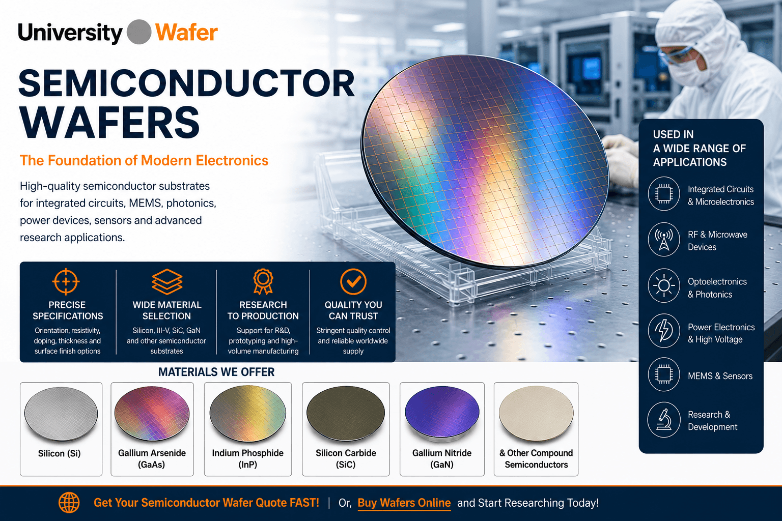
A semiconductor wafer is a thin, typically crystalline substrate used as the foundation for fabricating electronic, photonic, and microscale devices. During device fabrication, wafers can undergo processes such as thin-film deposition, photolithography, doping, ion implantation, oxidation, etching, and metallization to create functional structures on or within the substrate.
Silicon (Si) is the most widely used semiconductor substrate because of its mature manufacturing infrastructure, useful electrical properties, mechanical stability, and ability to form a high-quality native oxide (SiO2). However, other semiconductor materials are selected when an application requires properties that silicon cannot provide efficiently.
Silicon Semiconductor Wafers
Single-crystal silicon wafers are widely used for integrated circuits, discrete electronic devices, MEMS, sensors, photovoltaics, and materials research. Silicon substrates are available with different electrical and crystallographic properties to support specific fabrication requirements.
Silicon can be intentionally doped to produce p-type or n-type material. Common dopants include boron for p-type silicon and phosphorus, arsenic, or antimony for n-type silicon. The dopant species and concentration influence carrier concentration and electrical resistivity.
Silicon wafers may also be produced using different crystal-growth methods. Czochralski (CZ) silicon is widely used in semiconductor manufacturing, while Float Zone (FZ) silicon can provide very high resistivity and relatively low oxygen content for applications that require those characteristics.
Compound Semiconductor Wafers
Some applications require semiconductor properties beyond those available from silicon. Compound semiconductor wafers combine elements from different groups of the periodic table and can provide characteristics such as direct bandgaps, high electron mobility, wide bandgaps, or high breakdown fields.
Gallium arsenide (GaAs) is a direct-bandgap III-V semiconductor used in applications including RF electronics, optoelectronics, lasers, LEDs, detectors, and high-efficiency photovoltaic devices. Its electron mobility is substantially higher than that of silicon under comparable low-field conditions, making GaAs useful for certain high-frequency devices.
Indium phosphide (InP) is another direct-bandgap III-V material used extensively in photonics and high-speed optoelectronics, including devices for optical communications. InP can also serve as a substrate for epitaxial structures containing materials such as InGaAs.
Wide-Bandgap Semiconductor Materials
Silicon carbide (SiC) and gallium nitride (GaN) are important wide-bandgap semiconductor materials. Their large bandgaps and high critical electric fields make them attractive for applications involving high voltage, high power density, elevated temperature, and high-frequency operation.
SiC is particularly important for power semiconductor devices because it combines a wide bandgap with high thermal conductivity and a high critical electric field. GaN is widely used in RF and power electronics and, because of its direct bandgap, is also important for optoelectronic devices such as LEDs and laser diodes.
Important Semiconductor Wafer Specifications
Selecting the correct wafer requires more than choosing a semiconductor material. Researchers and device engineers should consider specifications that can influence both fabrication compatibility and final device performance.
- Material: Si, Ge, GaAs, InP, SiC, GaN, or another semiconductor appropriate for the application.
- Crystal Orientation: Orientations such as <100>, <110>, and <111> can influence surface structure, epitaxial growth, etching behavior, and device processing.
- Conductivity Type: P-type, n-type, semi-insulating, intrinsic, or nominally undoped material may be required depending on the semiconductor and application.
- Resistivity: Electrical resistivity is related to carrier concentration and mobility and is an important specification for many electronic, RF, detector, and research applications.
- Wafer Diameter and Thickness: These dimensions must be compatible with fabrication equipment, handling requirements, and the intended experiment.
- Surface Finish: Single-side polished (SSP), double-side polished (DSP), epi-ready, or other finishes can be selected according to the required process.
- Wafer Grade: Prime, test/monitor, mechanical, reclaimed, and other grades can serve different fabrication, equipment-development, or research requirements.
Choosing the Right Semiconductor Substrate
There is no single semiconductor wafer that is optimal for every device. Material selection depends on factors such as bandgap, carrier mobility, thermal conductivity, lattice parameters, electrical resistivity, optical properties, mechanical characteristics, and process compatibility.
For example, silicon dominates conventional integrated-circuit fabrication, while GaAs and InP are important for selected RF and photonic applications. SiC and GaN provide advantages for many high-power and high-field devices. The substrate specification should therefore be matched to both the desired material properties and the fabrication process.
Get Your Semiconductor Wafer Quote FAST!
Or,
Buy Wafers Online and Start Researching Today!
How Semiconductor Wafers Become Devices
A semiconductor wafer provides the starting platform for many electronic and photonic devices. During fabrication, carefully controlled processes create patterned regions, thin films, junctions, contacts, and interconnects on or within the wafer.
Depending on the device, fabrication can involve photolithography, oxidation, thin-film deposition, epitaxial growth, doping, ion implantation, wet or dry etching, and metallization. Multiple processing cycles can be used to build complex structures before individual devices are separated from the wafer by dicing.
Why Wafer Surface Quality Matters
Surface condition is an important consideration in semiconductor processing. Particles, scratches, contamination, crystal defects, and excessive surface roughness can interfere with lithography, thin-film deposition, epitaxial growth, bonding, and other fabrication steps.
For demanding applications, researchers may specify prime-grade, double-side polished (DSP), or epi-ready wafers. The appropriate finish depends on the intended process. For example, an epi-ready surface requires careful control of polishing, cleanliness, surface damage, and contamination to support high-quality epitaxial growth.
Doping, Resistivity and Electrical Properties
The electrical behavior of a semiconductor can be modified through doping, in which controlled concentrations of impurity atoms are introduced into the material. In silicon, acceptor dopants such as boron are commonly used to produce p-type material, while donor dopants such as phosphorus, arsenic, and antimony can produce n-type material.
Wafer resistivity is related to carrier concentration and carrier mobility. Heavily doped semiconductor material generally has lower resistivity than lightly doped material of the same type, although the exact relationship depends on dopant species, concentration, temperature, and carrier mobility.
High-resistivity and semi-insulating substrates can be useful when electrical isolation or reduced substrate-related losses are important, while lower resistivity wafers may be appropriate when the substrate is intended to participate in electrical conduction.
Semiconductor Wafers for Epitaxial Growth
Epitaxy is the growth of a crystalline layer whose structure is related to that of the underlying crystalline substrate. Epitaxial layers allow researchers and device manufacturers to engineer properties such as composition, doping, thickness, and heterostructure design.
Substrate selection for epitaxy requires consideration of factors such as crystal orientation, lattice compatibility, surface preparation, thermal expansion, defect density, and process temperature. Depending on the material system, epitaxial films can be deposited using techniques such as chemical vapor deposition (CVD), metal-organic chemical vapor deposition (MOCVD), or molecular beam epitaxy (MBE).
Wafers for Microelectronics and Integrated Circuits
Silicon remains the dominant substrate for conventional integrated circuits (ICs). Its established processing technology and ability to form high-quality silicon dioxide have contributed to its widespread use in CMOS and other semiconductor technologies.
During integrated-circuit fabrication, many devices are patterned across a single wafer. After fabrication and testing, the wafer can be diced into individual dies that are subsequently packaged for use in electronic systems.
Semiconductor Wafers for Photonics and Optoelectronics
III-V semiconductor materials are particularly important in optoelectronics because many have direct bandgaps that enable efficient interaction with light. GaAs and InP-based material systems are used in applications including laser diodes, photodetectors, LEDs, high-speed optical communication, and integrated photonics.
Silicon is also an important platform for integrated photonics, particularly for waveguides and electronic-photonic integration. Different material systems can also be combined through epitaxy, wafer bonding, or other heterogeneous integration techniques to obtain properties unavailable from a single material.
Wafers for Power and RF Electronics
Silicon carbide (SiC) and gallium nitride (GaN) are widely studied and used for power and high-frequency electronics. Their wide bandgaps and high critical electric fields enable device designs suited to higher electric fields than conventional silicon devices.
SiC also offers high thermal conductivity, which is advantageous for thermal management in high-power devices. GaN-based heterostructures are important for high-electron-mobility transistors (HEMTs) used in RF and power applications. The best material depends on operating voltage, frequency, temperature, thermal-management requirements, device architecture, and cost.
Semiconductor Wafers for MEMS and Sensors
Semiconductor wafers are also used to fabricate microelectromechanical systems (MEMS) and sensors. Silicon is especially important in MEMS because its mechanical properties can be combined with mature microfabrication techniques to create structures such as membranes, beams, resonators, and microchannels.
Wafer thickness, crystal orientation, surface finish, resistivity, and mechanical properties can all be important when selecting substrates for MEMS and sensor fabrication.
Semiconductor Wafer Characterization
Wafer characterization helps determine whether a substrate meets the requirements of a particular experiment or fabrication process. Depending on the material and application, measurements can include thickness, total thickness variation (TTV), bow, warp, surface roughness, resistivity, carrier concentration, crystal orientation, and defect density.
Techniques such as four-point probe measurements, Hall-effect measurements, atomic force microscopy (AFM), optical profilometry, X-ray diffraction (XRD), and ellipsometry can provide different types of electrical, structural, surface, and thin-film information. Not every technique is appropriate for every wafer, so characterization should be selected according to the material and property being investigated.
Matching the Wafer to Your Application
Selecting a semiconductor wafer requires balancing the properties of the substrate with the requirements of the fabrication process and final device. Important factors can include bandgap, carrier transport, thermal conductivity, breakdown field, optical response, crystal structure, resistivity, surface quality, wafer dimensions, and compatibility with subsequent processing.
Silicon is an excellent general-purpose platform for many semiconductor technologies, but compound and wide-bandgap semiconductors can provide important advantages for specific RF, photonic, power, sensing, and optoelectronic applications. Choosing the substrate based on the actual device requirements is therefore more useful than treating one semiconductor material as universally superior.
Related Semiconductor Wafer Resources
- Silicon Wafers – Explore silicon substrates by orientation, resistivity, doping, diameter, and surface finish.
- III-V Semiconductor Wafers – Explore III-V semiconductor materials for photonics, optoelectronics, RF devices, and advanced research.
- Gallium Arsenide (GaAs) Wafers – Learn about GaAs substrates for RF electronics, optoelectronics, detectors, and photovoltaic research.
- Indium Arsenide (InAs) Wafers – Explore narrow-bandgap InAs substrates for infrared, high-mobility, and semiconductor research.
- Silicon Carbide (SiC) Wafers – Explore wide-bandgap SiC substrates for power electronics, high-temperature devices, and research.
- Gallium Nitride (GaN) on Sapphire – Learn about GaN-on-sapphire structures for optoelectronics, LEDs, and semiconductor research.
- Molecular Beam Epitaxy (MBE) – Learn how MBE is used to grow controlled crystalline semiconductor layers and heterostructures.
- MOCVD Semiconductor Growth – Explore metal-organic chemical vapor deposition for III-V and compound semiconductor epitaxy.
- Atomic Force Microscopy (AFM) – Learn how AFM is used to characterize semiconductor wafer surfaces and nanoscale roughness.
- Chemical Mechanical Polishing (CMP) – Explore wafer planarization and surface preparation for semiconductor processing.