
How Does a MOCVD Reactor Work?
A MOCVD reactor creates thin crystalline semiconductor layers by delivering carefully controlled precursor gases over a heated substrate. MOCVD stands for Metal-Organic Chemical Vapor Deposition and is also commonly referred to as MOVPE (Metal-Organic Vapor Phase Epitaxy). The process is particularly important for producing high-quality III-V compound semiconductor epitaxial layers.
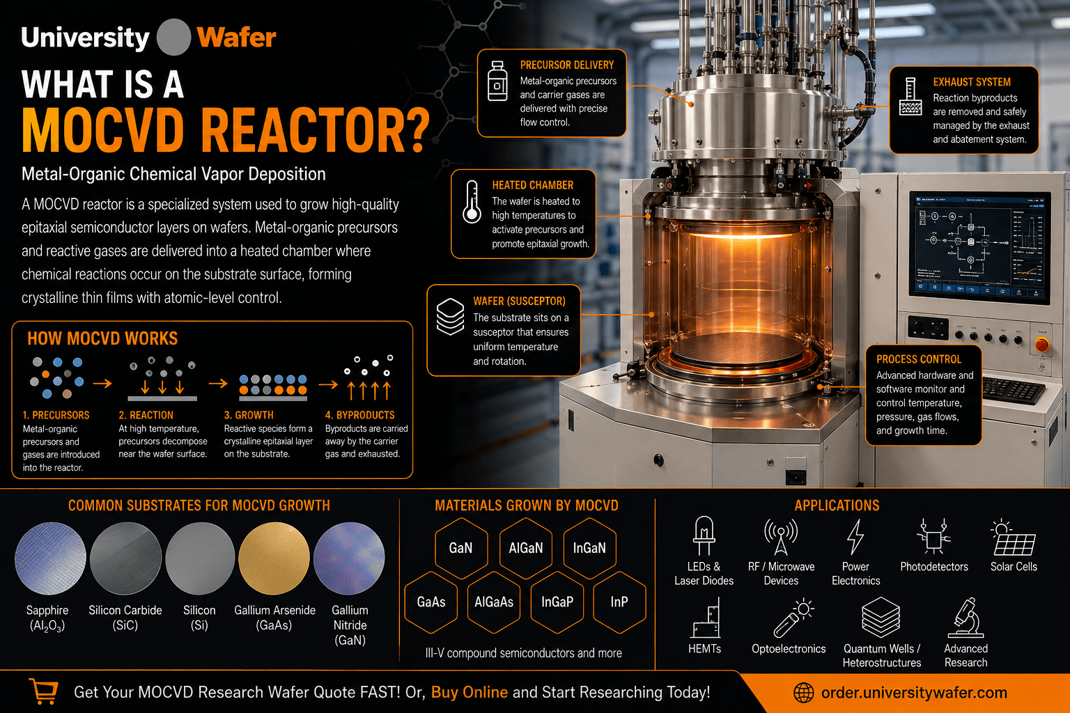
During deposition, metal-organic precursors and other source gases enter the reactor through a controlled gas-delivery system. When these precursors reach the heated wafer surface, chemical reactions and decomposition processes supply the atomic species needed for crystal growth. Reaction byproducts are then carried away through the reactor exhaust.
Main Components of a MOCVD Reactor
A modern MOCVD system combines several components that precisely control precursor delivery, wafer temperature, pressure, and gas flow. Maintaining stable process conditions is essential for achieving reproducible epitaxial thickness, composition, doping, and interface quality.
- Reaction Chamber: The controlled environment where semiconductor epitaxial growth takes place.
- Substrate Holder or Susceptor: Supports the wafer and helps maintain a controlled substrate temperature during growth.
- Heating System: Raises the substrate to the temperature required for precursor decomposition and crystal growth.
- Precursor Delivery System: Delivers metal-organic compounds and other process gases at controlled flow rates.
- Mass Flow Controllers: Precisely regulate the flow of carrier and reactant gases entering the reactor.
- Pressure Control System: Maintains the desired reactor pressure throughout the deposition process.
- Exhaust and Abatement System: Removes reaction byproducts and handles process gases after they leave the chamber.
What Materials Can Be Grown by MOCVD?
MOCVD is especially valuable for the growth of compound semiconductor materials. By changing precursor chemistry and process conditions, researchers can grow binary, ternary, and quaternary semiconductor alloys with carefully engineered compositions.
Common MOCVD-grown materials include:
- Gallium Nitride (GaN)
- Gallium Arsenide (GaAs)
- Aluminum Gallium Nitride (AlGaN)
- Indium Gallium Nitride (InGaN)
- Indium Phosphide (InP)
- Indium Gallium Phosphide (InGaP)
- Aluminum Gallium Arsenide (AlGaAs)
- Other III-V semiconductor alloys and heterostructures
MOCVD Precursors and Carrier Gases
MOCVD processes use volatile chemical compounds to transport the elements required for semiconductor growth. Metal-organic compounds are commonly used as Group III sources, while hydride or other suitable precursors can provide Group V elements.
For example, gallium-containing metal-organic precursors may be combined with a nitrogen source during GaN epitaxial growth. Carrier gases transport these precursors through the delivery system and into the reactor. The exact chemistry depends on the semiconductor composition and desired epitaxial structure.
Why Is Temperature Important in MOCVD?
Substrate temperature is one of the most important MOCVD process parameters. Temperature influences precursor decomposition, surface diffusion, incorporation efficiency, crystal quality, composition, and growth rate.
Precise temperature control is especially important when growing complex heterostructures containing multiple semiconductor layers. Even relatively small process changes can influence material properties, making repeatable temperature measurement and control essential for research and manufacturing.
Epitaxial Growth and Crystal Orientation
In epitaxial growth, the deposited crystalline layer develops an ordered relationship with the underlying substrate. For this reason, substrate material, crystal orientation, surface preparation, lattice parameters, and thermal properties can all affect the resulting epitaxial structure.
Researchers select substrates according to the material system being grown and the requirements of the final device. Silicon, sapphire, silicon carbide, gallium arsenide, gallium nitride, and other crystalline substrates may be used depending on the MOCVD application.
What Is a MOCVD Heterostructure?
One major advantage of MOCVD is its ability to deposit multiple semiconductor layers with different compositions. These structures are known as heterostructures. Process gases can be changed during growth to create controlled interfaces between materials with different electronic and optical properties.
MOCVD heterostructures can include buffer layers, barrier layers, quantum wells, active regions, and doped semiconductor layers. This level of control enables researchers to engineer materials for specific electrical, optical, and mechanical properties.
Applications of MOCVD Epitaxy
MOCVD has become an important deposition technology for both semiconductor research and high-volume manufacturing. Its ability to produce controlled compound semiconductor layers makes it particularly valuable for optoelectronic and high-performance electronic devices.
- LEDs and micro-LED research
- Laser diodes
- GaN power electronics
- RF and microwave devices
- High-electron-mobility transistors (HEMTs)
- Photodetectors
- Photonic and optical devices
- III-V solar cells
- Quantum wells and heterostructures
- Advanced semiconductor materials research
Substrate Quality for MOCVD Research
The quality of the starting substrate can significantly influence MOCVD epitaxial growth. Researchers may need to consider crystal orientation, wafer diameter, surface roughness, thickness, resistivity, defect density, polarity, offcut angle, and surface preparation when selecting substrates for epitaxy.
High-quality research wafers provide a controlled starting surface for studying nucleation, lattice mismatch, buffer-layer development, thin-film properties, and semiconductor device performance. Selecting the appropriate substrate is therefore an important part of designing a successful MOCVD experiment.
Get Your MOCVD Research Wafer Quote FAST! Or, buy online and start researching today!
MOCVD vs. CVD: What Is the Difference?
MOCVD is a specialized form of Chemical Vapor Deposition (CVD) designed primarily for the controlled epitaxial growth of compound semiconductors. While conventional CVD processes can deposit many types of films, MOCVD uses metal-organic precursors to supply elements needed to form crystalline semiconductor layers.
This precise control makes MOCVD particularly useful for growing gallium arsenide (GaAs) wafers and epitaxial structures , GaN, AlGaN, InGaN, InGaP, and other III-V semiconductor materials used in advanced electronics and photonics.
MOCVD Growth of Gallium Nitride (GaN)
GaN MOCVD is widely used to produce epitaxial layers for LEDs, laser diodes, RF electronics, and high-power semiconductor devices. GaN layers may be grown on several substrate materials depending on the research objective and desired device architecture.
Gallium nitride (GaN) wafers are particularly important for wide-bandgap semiconductor research. Researchers also investigate GaN growth on sapphire, silicon carbide, and silicon substrates to balance crystal quality, thermal performance, wafer size, and cost.
Sapphire Substrates for MOCVD
Sapphire wafers are commonly used as substrates for III-nitride epitaxy. Their thermal stability, electrical insulation, and crystalline properties make sapphire useful for GaN-based LEDs, optoelectronics, and experimental semiconductor structures.
Crystal orientation is important because the exposed crystallographic plane can influence epitaxial growth. Researchers may select C-plane, A-plane, R-plane, or other sapphire orientations according to the material system and experimental requirements.
Silicon Carbide Substrates for MOCVD
Silicon carbide (SiC) wafers provide excellent thermal conductivity and are important substrates for wide-bandgap semiconductor research. SiC can be used as a platform for GaN epitaxy when thermal management and high-power operation are important.
GaN-on-SiC structures are particularly relevant to RF, microwave, and high-power electronics. Substrate polytype, orientation, surface preparation, and defect characteristics should be considered when designing an epitaxial growth experiment.
Silicon Substrates for MOCVD Growth
Silicon wafers provide another platform for compound-semiconductor epitaxy and experimental thin-film growth. Their availability in many diameters, orientations, resistivities, dopant types, and surface finishes makes silicon useful for a broad range of research projects.
Growing compound semiconductors on silicon can present challenges related to lattice mismatch and thermal expansion differences. Researchers may use nucleation layers, buffer structures, and carefully controlled MOCVD conditions to manage these differences.
Gallium Arsenide and III-V MOCVD Growth
Gallium arsenide (GaAs) is an important III-V semiconductor used in RF electronics, photonics, lasers, detectors, and high-efficiency photovoltaic research. MOCVD can be used to build sophisticated epitaxial structures on GaAs substrates by depositing layers with controlled composition and doping.
Materials such as AlGaAs and InGaP can be incorporated into multilayer structures to create heterojunctions, confinement layers, and other engineered semiconductor interfaces.
AlGaN and Wide-Bandgap Semiconductor Research
Aluminum gallium nitride (AlGaN) is a wide-bandgap III-V semiconductor alloy frequently investigated alongside GaN. By adjusting aluminum composition during epitaxial growth, researchers can modify material properties for electronic and optoelectronic applications.
AlGaN/GaN heterostructures are especially important for high-electron-mobility transistor (HEMT) research and other high-frequency or high-power devices.
InGaP for Optoelectronic Applications
Indium gallium phosphide (InGaP) is another III-V compound semiconductor that can be incorporated into epitaxial device structures. InGaP is relevant to photonics, LEDs, heterojunction devices, and high-efficiency multijunction solar cells.
Precise control of precursor flow, substrate temperature, reactor pressure, and growth rate allows MOCVD researchers to engineer composition and layer thickness for complex III-V semiconductor structures.
MOCVD for Thin-Film and Epitaxial Research
MOCVD differs from many general thin-film deposition methods because it can produce highly controlled crystalline layers that follow the structure of an underlying substrate.
Researchers can adjust temperature, pressure, precursor ratios, carrier-gas flow, growth time, and substrate conditions to investigate how each variable affects film composition, morphology, crystal quality, and electrical or optical performance.
Surface Preparation Before MOCVD
Substrate preparation can strongly influence nucleation and epitaxial quality. Particles, organic contamination, native oxides, and other surface residues may interfere with the initial stages of film growth.
Appropriate silicon wafer cleaning and substrate preparation procedures can help create a controlled starting surface. The exact cleaning method should be selected for the substrate material and MOCVD chemistry being investigated.
Choosing Wafers for MOCVD Experiments
Selecting a substrate for MOCVD epitaxial growth requires more than choosing the base material. Researchers should consider crystal orientation, lattice compatibility, surface finish, wafer thickness, diameter, electrical properties, thermal characteristics, and the intended epitaxial structure.
UniversityWafer supplies semiconductor and crystalline substrates for MOCVD, epitaxy, thin-film deposition, device fabrication, and materials characterization research. Substrates can be selected according to the specific requirements of GaN, GaAs, AlGaN, InGaP, SiC, silicon, and other advanced material systems.