
Sapphire Wafers for Advanced Research
UniversityWafer supplies sapphire wafers (Al2O3) for semiconductor, optical, RF, MEMS, and materials science research. Sapphire combines excellent mechanical strength, thermal stability, electrical insulation, and optical transparency, making it a versatile substrate for demanding fabrication and laboratory applications.
Sapphire Substrates for GaN Research
Sapphire is widely used as a substrate for GaN on sapphire research. Its properties make it useful for studying epitaxial layers and developing LEDs, optoelectronic devices, sensors, and other semiconductor structures.
Sapphire Wafer Applications
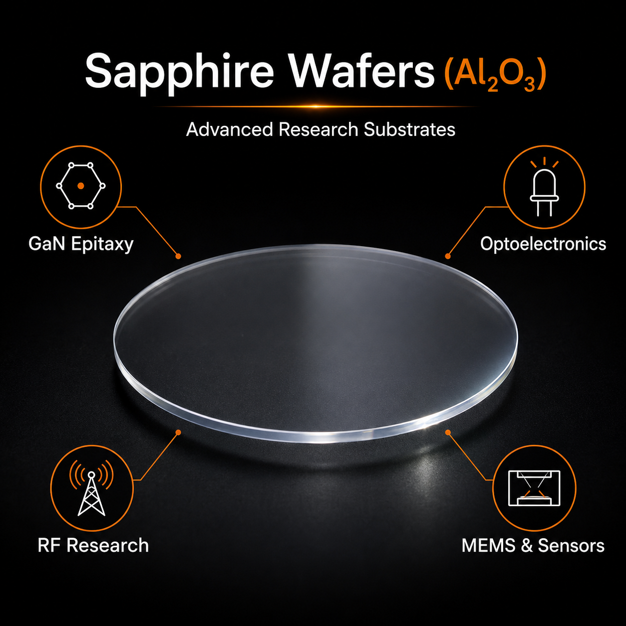
- GaN epitaxy: substrate research for gallium nitride films and devices.
- Optoelectronics: LEDs, photonics, and optical device development.
- RF research: electrically insulating substrates for high-frequency devices.
- MEMS: durable substrates for microsystems and sensor research.
- Thin-film deposition: substrates for coatings and experimental material layers.
- Optical research: transparent substrates for optical and photonic experiments.
Choose the Right Sapphire Wafer
Sapphire wafers can be specified by diameter, thickness, crystal orientation, and surface finish. Researchers may require C-plane, A-plane, R-plane, or M-plane sapphire depending on the intended experiment and epitaxial process. UniversityWafer can help source substrates that meet your specific research requirements.
Need Sapphire Wafers for Your Research?
Tell us your required diameter, orientation, thickness, surface finish, and quantity so we can help identify the appropriate sapphire substrate for your project.
Get Your Sapphire Wafer Quote FAST! Or Buy Online and Start Researching Today!
Sapphire Wafers for Semiconductor and Optical Research
Sapphire (Al2O3) wafers provide a stable, electrically insulating crystalline platform for semiconductor, optical, photonic, and thin-film research. Their combination of mechanical strength, thermal stability, and optical transparency makes sapphire substrates useful for demanding fabrication and characterization processes.
GaN Epitaxy on Sapphire
Sapphire is widely used for gallium nitride (GaN) epitaxy. Researchers use GaN on sapphire wafers to investigate LEDs, photodetectors, power electronics, RF devices, and other compound-semiconductor technologies.
Sapphire Crystal Orientations
Selecting the appropriate crystal orientation is important because it can influence epitaxial growth and device fabrication. Common sapphire orientations used in research include:
- C-Plane (0001): commonly used for GaN epitaxy, LEDs, and optoelectronic research.
- A-Plane: used for specialized epitaxial growth and optical applications.
- R-Plane: useful for thin-film, semiconductor, and materials research.
- M-Plane: investigated for nonpolar epitaxial growth and advanced GaN research.
Researchers interested in nonpolar orientations can learn more about M-plane sapphire wafers.
Applications of Al2O3 Wafers
- Semiconductor research: substrates for epitaxial films and experimental devices.
- LED research: substrate development for GaN-based light-emitting devices.
- RF electronics: electrically insulating platforms for high-frequency device research.
- Photonics: optical and optoelectronic device development.
- MEMS: durable substrates for sensors and microsystems.
- Thin-film deposition: crystalline surfaces for deposited materials and coatings.
Silicon on Sapphire Research
Sapphire is also the insulating foundation used in silicon-on-sapphire (SOS) wafers. SOS structures are valuable for research involving electrically isolated silicon devices, RF electronics, sensors, and specialized microelectronics.
Selecting Sapphire Wafers
When ordering sapphire substrates, consider wafer diameter, thickness, crystal orientation, surface finish, and quantity. UniversityWafer can help researchers source sapphire wafers appropriate for epitaxy, optical experiments, thin-film deposition, and semiconductor device development.