
Fused Silica Wafers for Research
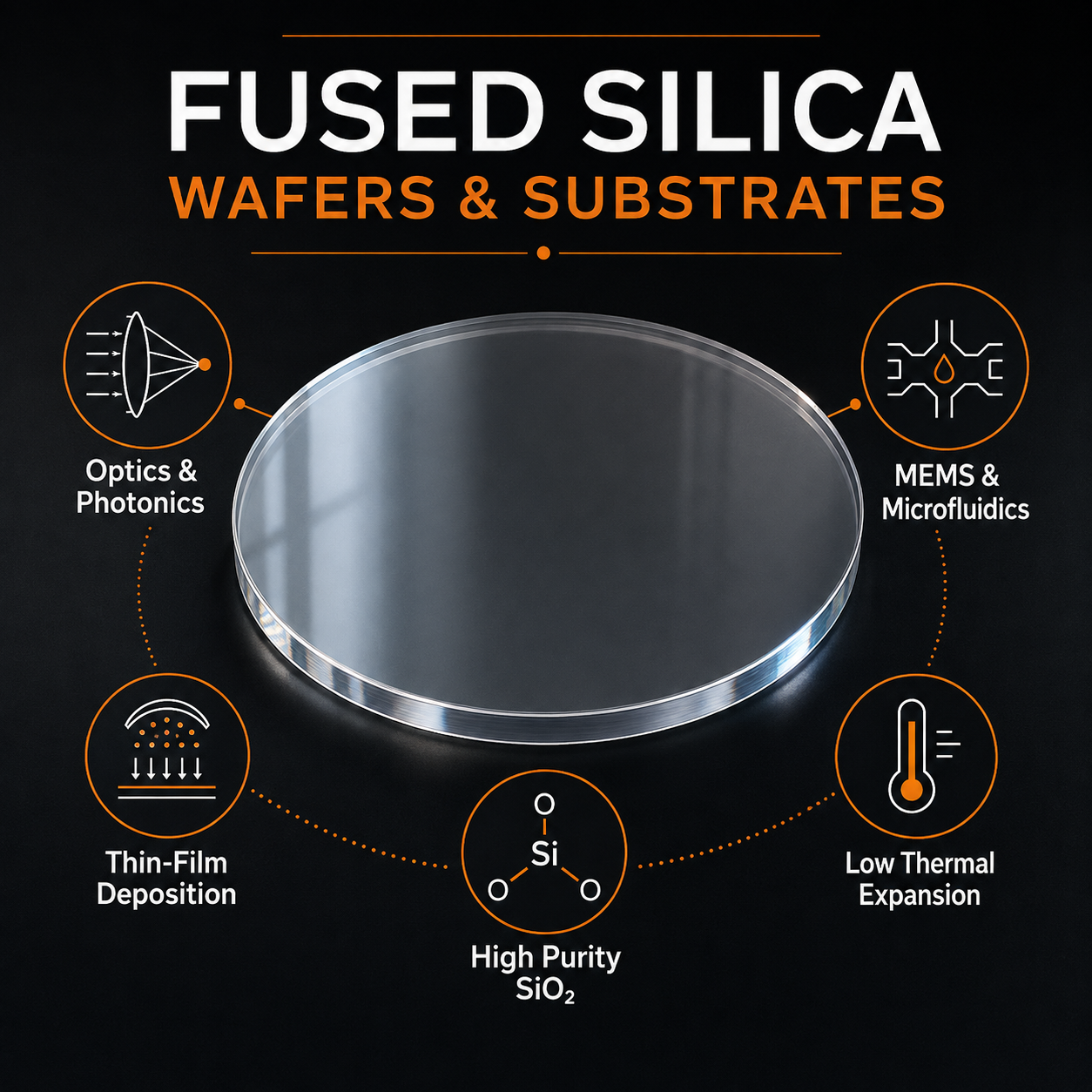
Fused silica wafers are high-purity amorphous silicon dioxide (SiO2) substrates used in optical, photonic, semiconductor, MEMS, and materials-science research. Their combination of optical transparency, thermal stability, and chemical resistance makes them suitable for demanding laboratory and fabrication processes.
Key Properties of Fused Silica
- High optical transparency across a broad wavelength range
- Low thermal expansion for dimensional stability
- High chemical purity for sensitive research applications
- Excellent thermal stability for elevated-temperature processing
- Electrical insulation for electronic and sensor applications
- Good chemical resistance for laboratory processing
Fused Silica for Optics and Photonics
The optical properties of fused silica make these substrates useful for photonics, optical coatings, laser research, imaging, and sensor development. Polished surfaces can provide a suitable platform for thin-film coatings and precision optical experiments where surface quality and transparency are important.
MEMS and Microfluidic Applications
Fused silica substrates are also used in MEMS and microfluidics. Their transparency can enable optical observation of channels and structures, while their chemical and thermal properties support many experimental fabrication and characterization processes.
Thin-Film Deposition Research
Researchers can use fused silica wafers as substrates for thin-film deposition, including dielectric, optical, conductive, and experimental material layers. Applications include coating characterization, interface studies, sensors, and prototype device fabrication.
Common Fused Silica Applications
- Optics and photonics research
- Optical and dielectric coatings
- Thin-film deposition
- MEMS fabrication
- Microfluidic devices
- Laser and spectroscopy research
- Sensors and experimental devices
- Semiconductor process development
Selecting a Fused Silica Wafer
Important specifications can include diameter, thickness, surface finish, flatness, dimensional tolerance, and optical requirements. Selecting the appropriate specifications helps ensure compatibility with your deposition, lithography, bonding, optical, or microfabrication process.
Need Fused Silica Wafers?
Tell us your required wafer dimensions, thickness, surface finish, quantity, and intended application. UniversityWafer can help identify fused silica substrates suitable for your research.
Get Your Fused Silica Wafer Quote FAST! Or Buy Online and Start Researching Today!
Why Choose Fused Silica Wafers?
Fused silica wafers combine high optical transparency, excellent thermal stability, low thermal expansion, and high chemical purity. Unlike crystalline quartz, fused silica has an amorphous structure, making it useful for precision optics, photonics, MEMS, microfluidics, and semiconductor research.
Fused Silica vs. Quartz
Fused silica consists primarily of high-purity silicon dioxide (SiO2) in a non-crystalline structure. Crystalline quartz, by comparison, has an ordered crystal lattice. This distinction influences their optical, thermal, mechanical, and electrical properties and should be considered when selecting a substrate for research.
Optical and Photonic Applications
Fused silica is widely used as an optical substrate because of its transparency and dimensional stability. Researchers use fused silica wafers for optical coatings, photonic structures, laser experiments, spectroscopy, sensors, and other precision optical applications.
Fused Silica for MEMS and Microfluidics
The transparency and chemical resistance of fused silica make it valuable for MEMS and microfluidic devices. Transparent substrates allow researchers to observe channels, fluids, particles, and device structures during experiments and characterization.
Thin-Film Deposition on Fused Silica
Polished fused silica wafers provide a stable platform for thin-film deposition and coating research. Researchers can deposit dielectric, optical, conductive, semiconductor, and experimental materials to investigate film properties, interfaces, adhesion, and device performance.
Common Research Applications
- Optics and photonics
- Optical and anti-reflective coatings
- Laser and spectroscopy experiments
- Thin-film deposition
- MEMS fabrication
- Microfluidic devices
- Optical and chemical sensors
- Semiconductor process research
- Wafer bonding and microfabrication
Surface Finish and Wafer Processing
Surface quality can be particularly important for optical coatings, lithography, bonding, and thin-film fabrication. Depending on the application, researchers may require single-side polished (SSP) or double-side polished (DSP) fused silica substrates with controlled thickness, flatness, and surface quality.
Selecting the Right Fused Silica Substrate
When specifying a fused silica wafer, consider diameter, thickness, surface finish, flatness, dimensional tolerance, purity, and optical requirements. The appropriate specifications depend on whether the substrate will be used for optical experiments, deposition, lithography, bonding, MEMS, or microfluidics.
Fused Silica Wafers for Advanced R&D
UniversityWafer supplies fused silica wafers and substrates for universities, laboratories, prototype development, and advanced R&D. Contact us with your required dimensions, surface specifications, quantity, and application to identify a substrate suitable for your research.