Custom Sputtering Services for Thin Film Deposition
UniversityWafer provides precision sputtering services for silicon wafers, glass, sapphire, quartz, ceramics, and customer-supplied substrates. Our vacuum sputter deposition capabilities support research and production applications requiring conductive metals, dielectric coatings, nitrides, oxides, and custom thin films with excellent adhesion, uniformity, and repeatability. :contentReference[oaicite:0]{index=0}
Get Your Sputtering Service Quote FAST!
UniversityWafer provides precision sputtering services for
universities, research laboratories, semiconductor manufacturers, and
technology companies developing advanced electronic, photonic, MEMS, and
optoelectronic devices. Our Physical Vapor Deposition (PVD) processes produce
high-quality thin films with excellent adhesion, uniformity, and repeatability
across a wide variety of substrate materials.
Whether you require a single conductive metal layer, a dielectric coating, or a
custom multilayer thin-film stack, our engineering team can recommend the
appropriate deposition process, target material, film thickness, and substrate
preparation to meet your project's performance requirements.
Recent Research Inquiry
"Our research group is fabricating MEMS pressure sensors and requires
RF magnetron sputtering of a 200 nm platinum thin film over a
20 nm titanium adhesion layer on 100 mm silicon wafers.
Can you provide film thickness uniformity, substrate preparation options,
expected lead time, and pricing for prototype quantities?"
Available Sputtering Capabilities
- RF magnetron sputtering
- DC magnetron sputtering
- Reactive sputtering processes
- Metal, alloy, dielectric, and semiconductor thin films
- Single-layer and multilayer thin-film deposition
- Custom film thicknesses from nanometers to microns
- Wafer, glass, quartz, sapphire, ceramic, and customer-supplied substrates
- Prototype through production-scale processing
Applications
Our sputtered thin films support research and manufacturing in
microelectronics, MEMS fabrication, photonic devices, optical coatings,
biosensors, semiconductor packaging, quantum devices, power electronics,
solar cells, RF components, and advanced materials development.
Complete the quotation form with your substrate material, wafer diameter,
target material, desired film thickness, deposition method, quantity, and any
special processing requirements. Our thin-film specialists will respond quickly
with technical recommendations and a competitive quotation.
Get Your Quote FAST! Or,
Browse Research Substrates
to Start Your Project Today!
What Is Sputtering?
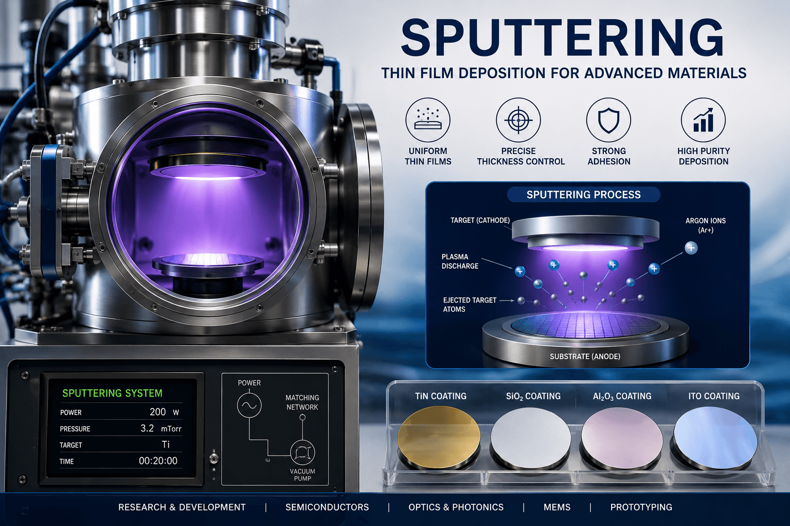
Sputtering is a Physical Vapor Deposition (PVD)
process used to deposit thin films of metals, dielectrics, alloys, and
semiconductor materials onto a substrate. During sputtering, energetic ions
strike a solid target, ejecting atoms that condense on the substrate to form a
uniform, highly adherent coating. The process provides excellent film
thickness control, repeatability, and material purity, making it one of the
most widely used deposition techniques in semiconductor manufacturing and
advanced materials research.
UniversityWafer offers custom sputtering services for silicon wafers, glass,
quartz, sapphire, ceramics, and other research substrates. Whether your project
requires a single conductive layer or a complex multilayer stack, our
engineering team can tailor the deposition process to meet your exact
specifications.
Sputtering Methods
| Process |
Advantages |
Typical Applications |
| DC Magnetron Sputtering |
High deposition rates for electrically conductive materials with excellent film uniformity. |
Metal contacts, seed layers, electrodes, and semiconductor metallization. |
| RF Magnetron Sputtering |
Ideal for insulating materials and dielectric coatings while maintaining excellent thickness control. |
Oxides, nitrides, optical coatings, MEMS, and photonic devices. |
| Reactive Sputtering |
Forms compound films by introducing reactive gases during deposition. |
Silicon nitride, metal oxides, transparent conductive films, and protective coatings. |
Materials Available for Sputtering
UniversityWafer can deposit a wide variety of thin-film materials for research
and commercial applications, including:
- Aluminum (Al)
- Gold (Au)
- Silver (Ag)
- Copper (Cu)
- Titanium (Ti)
- Chromium (Cr)
- Nickel (Ni)
- Platinum (Pt)
- Tungsten (W)
- Tantalum (Ta)
- Molybdenum (Mo)
- Silicon dioxide (SiO2)
- Silicon nitride (Si3N4)
- ITO and other transparent conductive oxides
- Custom metals, alloys, and compound thin films
Applications of Sputtered Thin Films
Sputtered coatings are widely used because they provide dense, durable, and
high-purity films suitable for demanding research and manufacturing
environments.
- Semiconductor device fabrication
- MEMS sensors and actuators
- Photonic integrated circuits
- Optical mirrors and anti-reflective coatings
- Solar cells and photovoltaic devices
- Quantum computing research
- Biomedical sensors
- RF and microwave electronics
- Microelectronics packaging
- Thin-film research and materials development
Custom Thin Film Deposition Services
Our sputtering services are available for prototype development through
production-scale manufacturing. We work closely with researchers and engineers
to optimize film composition, thickness, adhesion, uniformity, and substrate
compatibility for each application. Whether you need a simple metal coating or
a sophisticated multilayer thin-film structure, UniversityWafer can provide a
custom deposition solution designed to meet your technical requirements with
fast turnaround and consistent quality.
Related Thin Film Deposition Services
