
Silicon on Sapphire Wafers for Research
Silicon on Sapphire (SoS) is a semiconductor substrate consisting of a thin crystalline silicon layer formed on a sapphire (Al2O3) substrate. This combination provides researchers with the device-processing capabilities of silicon and the electrical insulation, mechanical strength, and stability of sapphire.
UniversityWafer supplies SoS wafers for university laboratories, semiconductor R&D, prototype fabrication, materials characterization, and advanced electronic device research.
Why Use Silicon on Sapphire?
Unlike conventional bulk silicon wafers, the silicon device layer in an SoS structure is electrically isolated from the supporting substrate. This can be advantageous for devices where substrate coupling, electrical isolation, and high-frequency performance are important.
- Excellent electrical isolation
- Reduced parasitic substrate effects
- Useful for high-frequency device research
- Strong and stable sapphire substrate
- Compatible with specialized CMOS processing
- Useful for RF and microwave electronics
- Suitable for radiation-effects research
SoS for RF and Microwave Research
RF (Radio Frequency) and microwave circuits can benefit from the insulating sapphire substrate because it helps reduce electrical interaction between the active silicon device layer and the underlying substrate.
SoS wafers can therefore support experimental devices for wireless communications, high-frequency integrated circuits, RF switches, microwave electronics, and other applications where researchers need good electrical isolation.
Silicon on Sapphire for CMOS
CMOS (Complementary Metal-Oxide-Semiconductor) devices can be fabricated in the thin silicon layer of an SoS wafer. The insulating sapphire underneath the silicon provides a device architecture that differs from conventional bulk-silicon CMOS.
Researchers can investigate transistor isolation, parasitic capacitance, device scaling, high-frequency behavior, and specialized integrated-circuit architectures using silicon-on-sapphire substrates.
SoS Wafer Specifications to Consider
Selecting an appropriate Silicon on Sapphire wafer depends on the fabrication process and intended device. Researchers may need to specify:
- Wafer diameter
- Silicon layer thickness
- Sapphire substrate thickness
- Silicon crystal orientation
- Sapphire orientation
- Silicon conductivity type
- Resistivity or doping requirements
- Surface finish
SoS for Radiation-Resistant Electronics
Silicon on Sapphire has also been investigated for electronics intended to operate in environments where radiation effects are important. The insulating substrate and isolated device regions make SoS useful for research into specialized electronics for aerospace, scientific instrumentation, and other demanding environments.
Silicon on Sapphire for MEMS and Sensors
SoS substrates can also support experimental MEMS (Micro-Electro-Mechanical Systems) and sensor technologies. Researchers can take advantage of the combination of a processable silicon layer and mechanically robust sapphire substrate when developing specialized microdevices.
Potential research areas include microsensors, high-temperature devices, RF MEMS, optical structures, and other devices that benefit from combining silicon electronics with sapphire.
Need a Specific Silicon on Sapphire Wafer?
Send UniversityWafer your required wafer diameter, silicon layer thickness, sapphire thickness, crystal orientation, doping, resistivity, and surface specifications. We can help identify an appropriate SoS substrate for your semiconductor research.
Get Your Silicon on Sapphire (SoS) Wafer Quote FAST! Or Buy Online and Start Researching Today!
What Is Silicon on Sapphire (SoS)?
Silicon on Sapphire (SoS) is a semiconductor material platform in which a crystalline silicon layer is grown on an electrically insulating sapphire (Al2O3) substrate. The silicon provides the active semiconductor layer for device fabrication, while sapphire provides electrical isolation and mechanical support.
SoS belongs to the broader family of silicon-on-insulator (SOI) technologies, although sapphire serves as the insulating substrate rather than the buried silicon dioxide layer commonly used in conventional SOI.
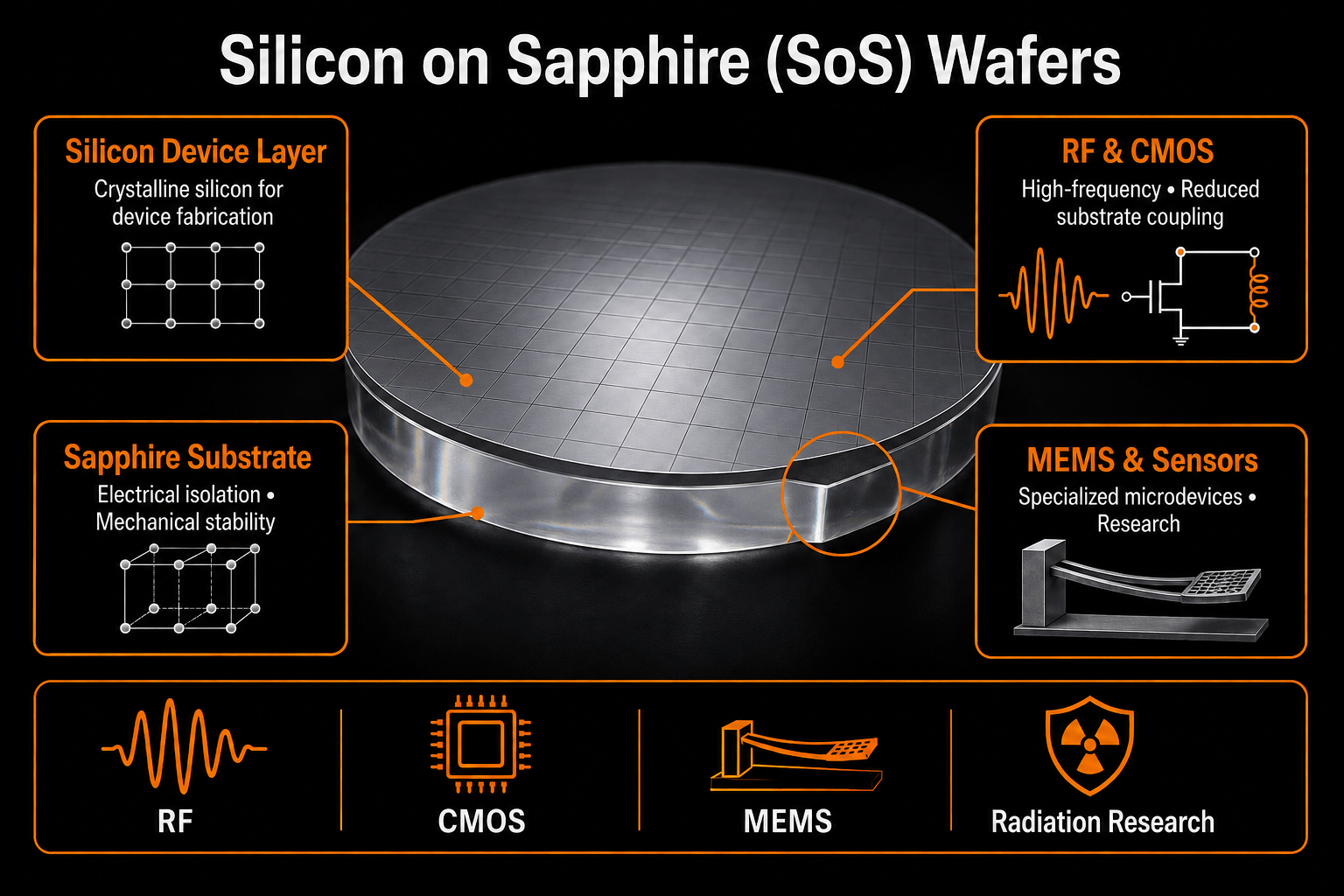
Silicon and Sapphire in One Substrate
Combining crystalline silicon with sapphire allows researchers to investigate devices that take advantage of properties from both materials.
- Silicon: established semiconductor processing and device fabrication
- Sapphire: electrical insulation and mechanical stability
- SoS: isolated silicon devices on a robust insulating substrate
SoS vs. Bulk Silicon
Conventional silicon wafers provide an excellent platform for semiconductor fabrication, while SoS offers additional electrical isolation for specialized device architectures.
| Property | Silicon on Sapphire | Bulk Silicon |
|---|---|---|
| Device Layer | Crystalline silicon | Bulk crystalline silicon |
| Supporting Substrate | Insulating sapphire | Silicon |
| Electrical Isolation | Excellent | More limited |
| Substrate Coupling | Reduced | Greater |
| Typical Research | RF, CMOS, radiation effects, sensors | CMOS, MEMS, ICs, general semiconductor devices |
SoS vs. Conventional SOI Wafers
Both SoS and conventional Silicon-on-Insulator (SOI) isolate the active silicon device region from the underlying substrate, but their structures are different.
Conventional SOI typically contains a silicon device layer, a buried oxide (BOX) layer, and a silicon handle wafer. In Silicon on Sapphire, the silicon device layer is instead supported by sapphire, eliminating the conventional silicon BOX/handle configuration.
High-Frequency Applications of SoS
One of the major research areas for Silicon on Sapphire involves RF and microwave electronics. Sapphire is electrically insulating, helping researchers reduce substrate-related parasitic effects that can influence high-frequency circuit performance.
- RF switches
- High-frequency transistors
- Microwave integrated circuits
- Wireless communication devices
- Mixed-signal electronics
- RF MEMS research
Radiation Effects and Aerospace Research
SoS technology has long been investigated for electronics operating in radiation-sensitive environments. Its isolated device structure makes the material useful for studying semiconductor behavior under conditions relevant to aerospace, space-based electronics, scientific instrumentation, and other specialized systems.
Silicon on Sapphire Research Applications
- RF and microwave semiconductor devices
- CMOS integrated circuits
- Radiation-effects research
- Aerospace electronics
- MEMS and microsensors
- High-frequency electronics
- Optoelectronic research
- Thin-film silicon device studies
- Material and interface characterization
Research-Grade SoS Substrates
UniversityWafer supplies semiconductor substrates for university laboratories, industrial R&D, prototype device fabrication, and materials research. Small quantities of Silicon on Sapphire wafers can support proof-of-concept experiments before researchers move to larger-scale fabrication.
Selecting the appropriate silicon thickness, crystal orientation, sapphire orientation, doping, and surface condition is important when matching an SoS wafer to a specific device fabrication process.