
High-Performance Silicon-on-Insulator (SOI) Wafers
Silicon-on-Insulator (SOI) wafers are engineered substrates designed to improve the electrical performance, speed, and energy efficiency of advanced semiconductor devices. By incorporating a buried oxide (BOX) layer between the silicon device layer and the silicon handle wafer, SOI technology significantly reduces parasitic capacitance, minimizes leakage currents, and enhances device isolation. UniversityWafer supplies premium SOI wafers for universities, research laboratories, semiconductor manufacturers, and MEMS developers worldwide.
Our SOI wafers are available with customizable device layer thicknesses, BOX layer thicknesses, wafer diameters, crystal orientations, doping types, resistivities, and polishing options. Whether you require ultra-thin device layers for silicon photonics or thicker silicon layers for MEMS fabrication, we can provide substrates tailored to your exact specifications.
Applications of SOI Wafers
- MEMS sensors and actuators
- CMOS integrated circuits
- RF switches and RF SOI technologies
- Silicon photonics and optical communications
- Power semiconductor devices
- Microfluidic devices
- Biosensors and biomedical devices
- Aerospace and radiation-hardened electronics
- Quantum technology research
- University and government laboratory research
Custom SOI Wafer Solutions
UniversityWafer offers custom SOI substrates manufactured to meet demanding research and production requirements. Available options include bonded SOI, layer-transfer SOI, and SIMOX technologies with configurable device layers, buried oxide thicknesses, handle wafer properties, crystal orientations, and surface finishes to support a wide range of semiconductor and MEMS applications.
Get Your Silicon-on-Insulator (SOI) Wafer Quote FAST! Or Buy Online and Start Researching Today!
Why Choose UniversityWafer?
For decades, UniversityWafer has been a trusted supplier of premium research substrates and engineered semiconductor materials. Our SOI wafers are manufactured to rigorous quality standards and backed by expert technical support, competitive pricing, fast quotations, and worldwide shipping, helping researchers and manufacturers accelerate innovation in MEMS, photonics, RF electronics, and advanced semiconductor technologies.
What Is a Silicon-on-Insulator (SOI) Wafer?
A Silicon-on-Insulator (SOI) wafer is an engineered substrate consisting of three primary layers: a thin silicon device layer, a buried oxide (BOX) layer, and a silicon handle wafer. The insulating BOX layer electrically isolates active devices from the substrate, reducing parasitic capacitance, minimizing power consumption, and improving switching speed. These advantages make SOI wafers ideal for high-performance semiconductor devices, MEMS, RF electronics, and silicon photonics.
SOI substrates are manufactured using advanced bonding and layer-transfer technologies that produce highly uniform silicon layers with excellent thickness control and superior surface quality. The result is a substrate that enables greater device reliability, improved thermal performance, and enhanced electrical isolation compared to conventional bulk silicon wafers.
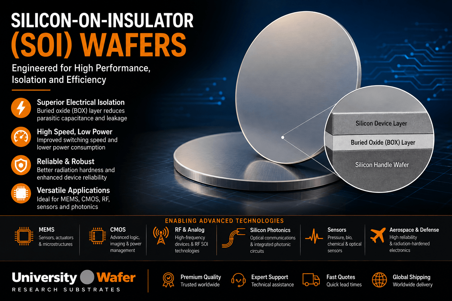
Typical SOI Wafer Structure
| Layer | Function |
|---|---|
| Silicon Device Layer | Forms the active semiconductor devices and integrated circuits. |
| Buried Oxide (BOX) | Provides electrical insulation, reduces parasitic capacitance, and improves device isolation. |
| Silicon Handle Wafer | Provides mechanical support and structural stability during fabrication. |
Advantages of SOI Wafers
- Excellent electrical isolation
- Lower parasitic capacitance and leakage currents
- Higher switching speeds
- Reduced power consumption
- Improved radiation resistance
- Superior thermal performance
- Ideal for high-frequency and RF applications
- Available with custom device and BOX layer thicknesses
Research & Industrial Applications
Silicon-on-insulator wafers are widely used in MEMS sensors, CMOS integrated circuits, RF switches, silicon photonics, microfluidic devices, power electronics, biosensors, optical communications, and aerospace electronics. Their unique layered structure enables the fabrication of smaller, faster, and more energy-efficient devices for both research laboratories and commercial semiconductor production.
UniversityWafer supplies premium research substrates, high-quality Silicon-on-Insulator (SOI) wafers, and custom engineered substrates with configurable device layers, buried oxide thicknesses, wafer diameters, crystal orientations, and resistivity specifications to support advanced semiconductor research and manufacturing.