
High-Quality TEOS Oxide Wafers for Advanced Research
TEOS oxide wafers are widely used throughout the semiconductor industry because they provide highly uniform silicon dioxide (SiO2) dielectric films with excellent electrical insulation and conformal coverage. Deposited using tetraethyl orthosilicate (TEOS) during chemical vapor deposition (CVD), these oxide layers are ideal for integrated circuits, MEMS devices, photonics, sensors, and advanced microelectronics research. UniversityWafer supplies premium TEOS-coated wafers manufactured to meet the demanding requirements of universities, research laboratories, and commercial semiconductor manufacturers.
Our TEOS oxide wafers are available with custom oxide thicknesses on a variety of substrates including silicon, silicon-on-insulator (SOI), quartz, fused silica, and other specialty materials. Films can be deposited using either PECVD or LPCVD processes depending on your application's electrical, mechanical, and thermal requirements.
Applications of TEOS Oxide Wafers
- CMOS and integrated circuit fabrication
- Shallow trench isolation (STI)
- Interlayer dielectric (ILD) deposition
- MEMS and microelectromechanical systems
- Chemical mechanical polishing (CMP)
- Sacrificial oxide layers
- Photonics and optical devices
- Microfluidic and biosensor fabrication
- Advanced packaging technologies
- University and government laboratory research
Custom Deposition Services
UniversityWafer offers custom TEOS deposition services with precisely controlled oxide thicknesses, wafer diameters, substrate materials, crystal orientations, and polishing specifications. Whether you require prototype quantities for research or larger production volumes, our technical team can help identify the ideal TEOS oxide solution for your project.
Get Your TEOS Oxide Wafer Quote FAST! Or Buy Online and Start Researching Today!
Why Choose UniversityWafer?
For decades, UniversityWafer has supplied premium research substrates, dielectric-coated wafers, and advanced semiconductor materials to customers around the world. Our TEOS oxide wafers are manufactured to rigorous quality standards and supported by expert technical assistance, fast quotations, competitive pricing, and worldwide shipping to help accelerate semiconductor innovation.
What Is a TEOS Oxide Wafer?
A TEOS oxide wafer is a silicon wafer coated with a thin film of silicon dioxide (SiO2) deposited using tetraethyl orthosilicate (TEOS) as the silicon precursor during chemical vapor deposition (CVD). TEOS oxide films are widely used because they provide excellent step coverage, uniform thickness, high dielectric strength, and reliable insulation between conductive layers. These characteristics make TEOS oxide one of the most commonly used dielectric materials in semiconductor manufacturing and MEMS fabrication.
Depending on the application, TEOS films are deposited using either Plasma-Enhanced Chemical Vapor Deposition (PECVD) for lower-temperature processing or Low-Pressure Chemical Vapor Deposition (LPCVD) when higher film density and superior electrical properties are required.
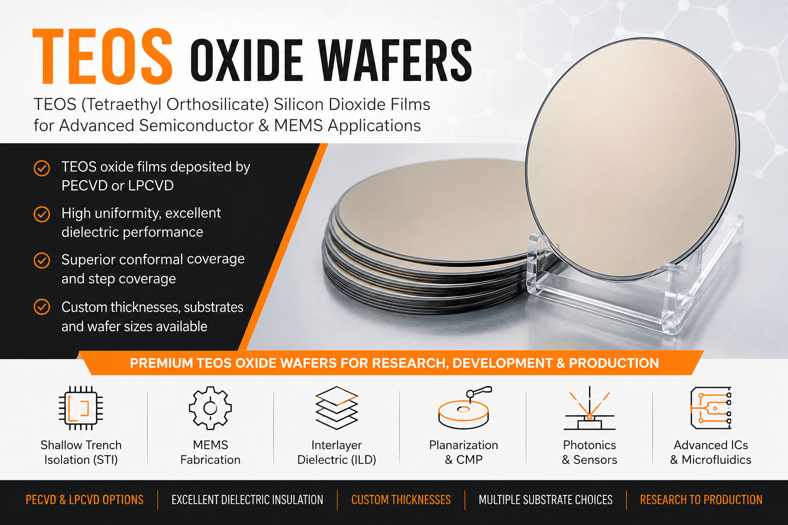
Common TEOS Oxide Applications
| Application | Purpose |
|---|---|
| Shallow Trench Isolation (STI) | Electrically isolates neighboring semiconductor devices on integrated circuits. |
| MEMS Fabrication | Serves as sacrificial layers and electrical insulation in MEMS structures. |
| Interlayer Dielectric (ILD) | Separates multiple metal interconnect layers within semiconductor devices. |
| Planarization & CMP | Provides uniform oxide films before chemical mechanical polishing. |
| Photonics & Sensors | Creates insulating and optical layers for integrated photonic and sensing devices. |
Advantages of TEOS Silicon Dioxide Films
- Excellent dielectric insulation
- Highly uniform oxide thickness
- Outstanding conformal coverage over complex structures
- Low defect density and high film quality
- Compatible with PECVD and LPCVD deposition processes
- Excellent adhesion to silicon substrates
- Supports advanced semiconductor manufacturing processes
- Available in custom oxide thicknesses and wafer sizes
Research & Industrial Applications
Researchers and semiconductor manufacturers use TEOS oxide wafers for integrated circuits, MEMS devices, CMOS fabrication, RF components, photonics, biosensors, microfluidic devices, and advanced packaging technologies. TEOS silicon dioxide continues to be one of the industry's preferred dielectric materials because of its excellent electrical performance, high process compatibility, and reliable long-term stability.
UniversityWafer supplies premium research substrates, high-quality TEOS oxide wafers, and custom silicon dioxide-coated wafers with a wide range of substrate materials, oxide thicknesses, wafer diameters, and polishing specifications to support semiconductor research and commercial production.