
Silicon Carbide Wafers for Research
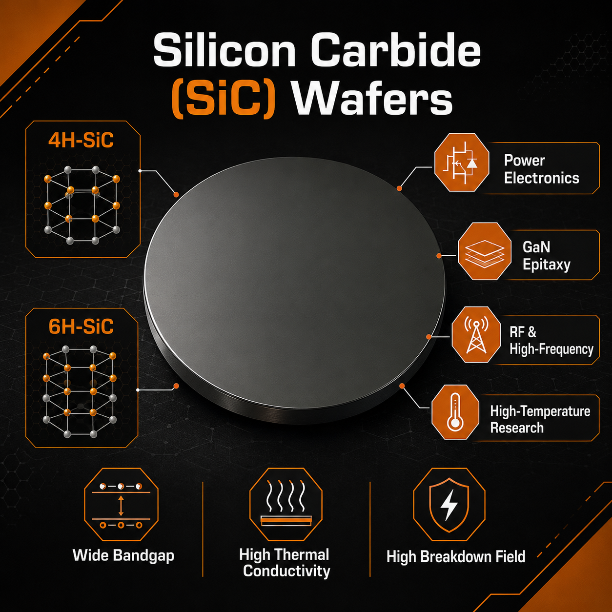
Silicon Carbide (SiC) wafers are widely used in advanced semiconductor research because of their wide bandgap, high thermal conductivity, high breakdown electric field, and ability to operate under demanding conditions. These properties make SiC an important substrate for next-generation power electronics, RF devices, sensors, and epitaxial research.
4H-SiC and 6H-SiC Substrates
Silicon carbide exists in several crystalline forms, or polytypes. 4H-SiC is widely used for power semiconductor research because of its favorable electronic properties, while 6H-SiC is also used in semiconductor, optical, and materials-science applications.
- 4H-SiC: widely used for power devices, MOSFETs, diodes, and high-frequency research
- 6H-SiC: used for semiconductor, optical, and materials research
- Semi-insulating SiC: useful for RF devices and GaN epitaxy
- Conductive SiC: suitable for power-electronic device development
Why Researchers Choose SiC
- Wide-bandgap semiconductor material
- High thermal conductivity
- High breakdown electric field
- Excellent high-temperature performance
- Suitable for high-power and high-frequency electronics
- Compatible with advanced epitaxial growth research
SiC for Power Electronics
4H-SiC wafers are particularly important for research into power MOSFETs, Schottky diodes, high-voltage devices, and other power-semiconductor technologies. SiC can support devices designed to operate at higher voltages and temperatures than conventional silicon-based technologies.
SiC for GaN Epitaxy
Silicon carbide substrates are also used for Gallium Nitride (GaN) epitaxy. Their thermal properties make SiC an attractive substrate platform for GaN-based high-frequency, RF, optoelectronic, and power-device research.
Common SiC Research Applications
- Power MOSFETs and Schottky diodes
- High-voltage semiconductor devices
- GaN epitaxial growth
- RF and microwave electronics
- MEMS and sensor research
- High-temperature electronics
- Wide-bandgap semiconductor research
Need a Specific SiC Wafer?
Tell us your required polytype, diameter, orientation, thickness, conductivity, doping, surface finish, and quantity. UniversityWafer can help identify Silicon Carbide substrates suitable for your research and fabrication requirements.
Get Your Silicon Carbide Wafer Quote FAST! Or Buy Online and Start Researching Today!
Why Use Silicon Carbide (SiC)?
Silicon Carbide (SiC) is a wide-bandgap semiconductor engineered for applications where high voltage, elevated temperature, and demanding power conditions can limit conventional silicon devices. Its electrical and thermal properties make SiC an important material for advanced semiconductor research and device development.
4H-SiC for Power Semiconductor Devices
4H-SiC wafers are widely used for power electronics research, including MOSFETs, Schottky barrier diodes, and high-voltage devices. The combination of a wide bandgap, high critical electric field, and good thermal conductivity enables researchers to investigate devices designed for efficient operation under demanding conditions.
Conductive vs. Semi-Insulating SiC
Selecting the correct electrical properties is important when specifying a SiC substrate. Conductive SiC wafers are commonly used for vertical power-device research, while semi-insulating SiC substrates provide electrical isolation useful for RF, microwave, and GaN-based device structures.
SiC Substrates for GaN Epitaxy
Silicon carbide is an important substrate for Gallium Nitride (GaN) epitaxial growth. GaN-on-SiC structures are studied for RF electronics, high-electron-mobility transistors (HEMTs), power devices, and other high-performance semiconductor technologies.
SiC Wafer Applications
- Power electronics and high-voltage devices
- SiC MOSFETs and Schottky barrier diodes
- GaN epitaxy and GaN-on-SiC structures
- RF and microwave electronics
- High-temperature semiconductor research
- MEMS and sensor development
- Wide-bandgap semiconductor research
- Thin-film and epitaxial material studies
Selecting the Right SiC Wafer
Important specifications include polytype, wafer diameter, crystal orientation, off-axis angle, thickness, doping, resistivity, conductivity, and surface finish. These parameters should be selected according to the intended epitaxy, fabrication, characterization, or device-development process.
Surface Finish and Epitaxy Preparation
Surface quality is especially important for processes such as epitaxial growth and semiconductor fabrication. Researchers should consider whether a substrate requires single-side or double-side polishing and whether the surface specifications are suitable for the planned deposition, lithography, oxidation, or epitaxial process.
Silicon Carbide Wafers for Advanced R&D
UniversityWafer supplies 4H-SiC, 6H-SiC, conductive, and semi-insulating Silicon Carbide substrates for universities, laboratories, semiconductor research, and prototype development. Substrate specifications can be selected to match a wide range of wide-bandgap semiconductor experiments and fabrication requirements.