
Ultrasonic Wafer Cleaning for Semiconductor Research
Ultrasonic cleaning is a surface-cleaning technique that uses high-frequency sound waves transmitted through a liquid cleaning solution. These sound waves create microscopic cavitation activity that can help dislodge particles, residues, oils, and other contaminants from silicon wafer surfaces.
For semiconductor and materials research, maintaining a clean wafer surface is important because contamination can interfere with subsequent processing steps. Proper silicon wafer cleaning can improve surface preparation before deposition, lithography, oxidation, bonding, microscopy, and other laboratory processes.
How Does Ultrasonic Cleaning Work?
An ultrasonic cleaner typically contains a liquid-filled tank and one or more transducers that convert electrical energy into high-frequency mechanical vibrations. These vibrations propagate through the cleaning liquid as pressure waves.
During this process, microscopic bubbles can form and collapse within the liquid. This phenomenon, known as acoustic cavitation, produces localized fluid motion that can help loosen contaminants attached to a wafer or substrate surface.
What Is Ultrasonic Cavitation?
Ultrasonic cavitation is central to the cleaning process. Alternating pressure cycles generated by ultrasonic waves can produce microscopic cavities or bubbles in the cleaning liquid. Their growth and collapse contribute to the mechanical cleaning action near exposed surfaces.
The effectiveness and aggressiveness of cavitation depend on several factors, including ultrasonic frequency, power, liquid properties, temperature, tank configuration, and the position of the sample.
Removing Particles from Silicon Wafers
Particles on a wafer surface can cause problems during semiconductor processing and surface characterization. Dust, polishing debris, handling contamination, and other particulate matter may interfere with photolithography, thin-film deposition, microscopy, or wafer bonding.
Ultrasonic cleaning can help remove loosely attached particles from silicon wafers without manually scrubbing the polished surface.
Removing Organic Residues and Contamination
Depending on the cleaning chemistry, ultrasonic agitation may also assist with removing oils, residues, and other surface contamination. The cleaning solution should be selected according to the substrate material and the type of contamination being removed.
Ultrasonic energy primarily provides mechanical agitation; it does not replace the chemical action required to dissolve or react with specific contaminants. For this reason, cleaning chemistry and ultrasonic parameters should be considered together.
Ultrasonic Cleaning Frequency
The ultrasonic frequency influences cavitation behavior and the mechanical action of the cleaning process. Lower frequencies generally produce more energetic cavitation, while higher frequencies can provide gentler cleaning action with smaller cavitation bubbles.
The appropriate frequency depends on the substrate, contamination level, and sensitivity of any structures already fabricated on the wafer.
Cleaning Solutions for Silicon Wafers
The liquid used during ultrasonic cleaning should be compatible with both the wafer and the contaminants being removed. Depending on the experiment, researchers may use high-purity water or an appropriate solvent or cleaning chemistry.
More extensive semiconductor cleaning processes may combine ultrasonic treatment with wafer surface cleaning methods designed to address particles, organic contamination, metallic impurities, or surface oxides.
Important Ultrasonic Cleaning Parameters
Researchers should control the cleaning conditions rather than treating ultrasonic cleaning as a single fixed process. Important parameters include:
- Ultrasonic frequency
- Ultrasonic power
- Cleaning time
- Cleaning-solution chemistry
- Solution temperature
- Wafer position in the tank
- Contamination type and concentration
- Wafer material and surface condition
Cleaning Before Thin-Film Deposition
A clean substrate is particularly important before depositing thin films. Surface contamination can influence nucleation, adhesion, morphology, uniformity, and interface quality.
Removing unwanted particles and residues before deposition provides researchers with a more controlled starting surface for experiments involving metals, dielectrics, semiconductors, polymers, and other thin-film materials.
Cleaning Before Photolithography
Particles and residues can also interfere with photolithography. Contamination may affect photoresist coating, exposure, pattern definition, or subsequent processing.
Appropriate wafer cleaning before lithography helps establish a cleaner surface for resist application and microfabrication experiments.
Ultrasonic Cleaning Before Wafer Bonding
Surface cleanliness is especially important for wafer bonding because particles trapped between two surfaces can prevent intimate contact and create local bonding defects.
Cleaning and surface preparation should therefore be carefully controlled when wafers will subsequently undergo direct bonding, adhesive bonding, anodic bonding, or another bonding process.
Cleaning Wafers for AFM and Surface Analysis
Contamination becomes particularly noticeable during nanoscale characterization. A particle that appears insignificant to the naked eye can become a major feature in an Atomic Force Microscopy scan.
Researchers using silicon wafers for Atomic Force Microscopy (AFM) should use appropriate cleaning and handling procedures to minimize particles and residues before surface measurements.
Protecting Low-Roughness Silicon Surfaces
Researchers working with low surface roughness silicon wafers should select cleaning conditions carefully. Excessively aggressive cleaning can be undesirable when the experiment depends on maintaining a highly controlled polished surface or when delicate structures are already present.
Cleaning parameters should therefore be optimized for the specific wafer, surface condition, and experimental objective.
When Should Ultrasonic Cleaning Be Used Carefully?
Although ultrasonic cleaning can be effective for bare wafers and robust substrates, it may not be appropriate for every sample. Strong cavitation and mechanical agitation can potentially affect fragile structures, membranes, patterned features, thin films, wire bonds, or other delicate components.
For sensitive samples, researchers should evaluate cleaning frequency, power, duration, chemistry, and alternative cleaning methods before processing valuable devices.
Applications of Ultrasonic Wafer Cleaning
- Particle removal from silicon wafers
- Surface preparation before thin-film deposition
- Cleaning before photolithography
- Wafer preparation before oxidation
- Surface preparation for wafer bonding
- MEMS and microfabrication research
- AFM and microscopy sample preparation
- Removal of polishing and handling residues
- Research substrate preparation
- General semiconductor laboratory cleaning
Start With the Right Silicon Wafer
Cleaning is only one part of substrate preparation. Wafer diameter, orientation, resistivity, thickness, surface finish, and initial surface quality should also be selected according to the intended semiconductor process.
UniversityWafer supplies silicon and other semiconductor substrates for cleaning studies, thin-film deposition, photolithography, MEMS, surface characterization, wafer bonding, and advanced materials research.
Get Your Silicon Wafer Quote FAST! Or, buy online and start researching today!
Ultrasonic Wafer Cleaning Process and Equipment
Effective ultrasonic wafer cleaning requires more than placing a substrate in an ultrasonic bath. Cleaning performance depends on the interaction between acoustic frequency, power, cleaning chemistry, temperature, exposure time, wafer position, and the type of contamination present on the surface.
For semiconductor research, these parameters should be controlled carefully to remove unwanted contamination while preserving the surface quality of silicon wafers and other sensitive substrates.
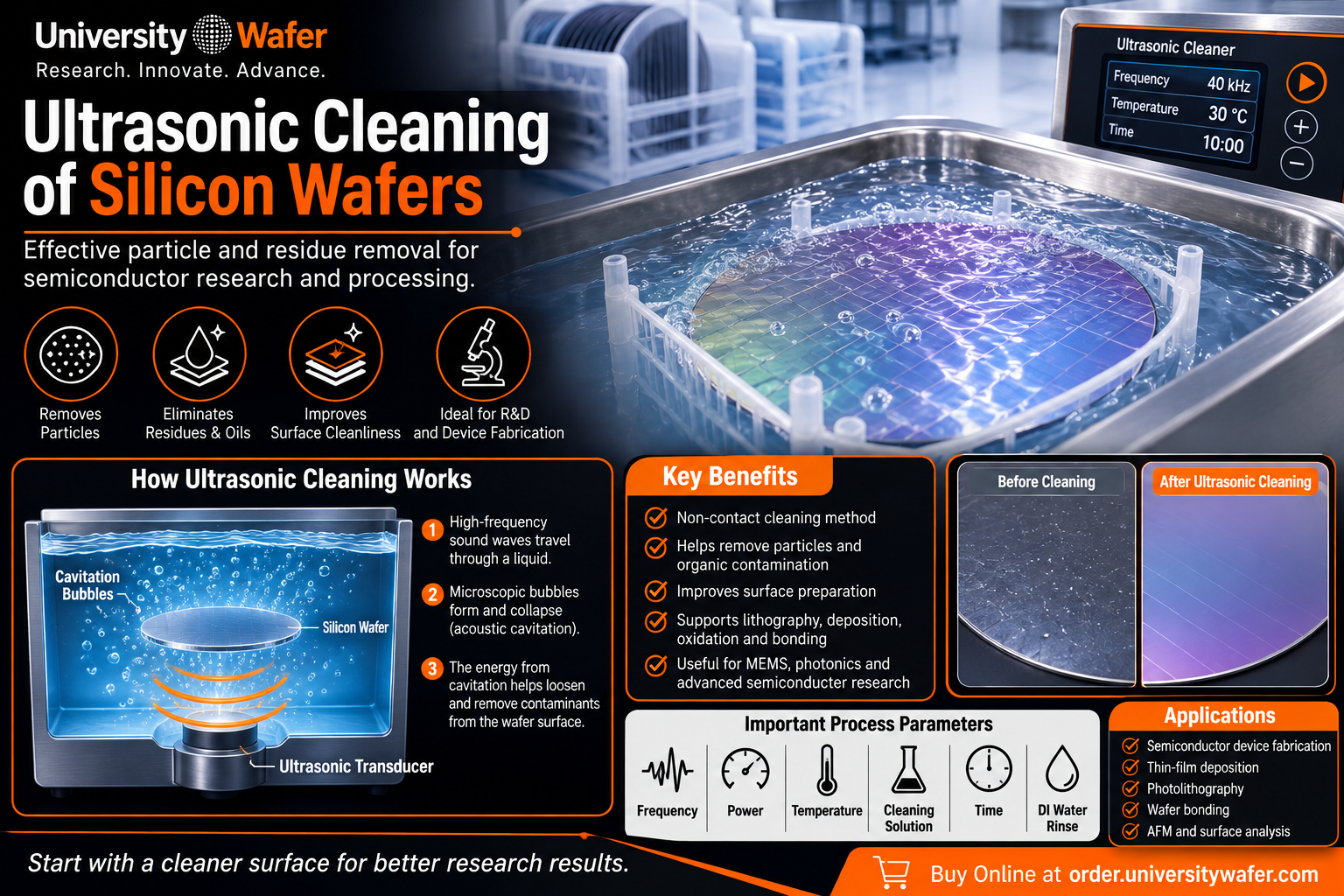
Components of an Ultrasonic Cleaning System
A laboratory ultrasonic cleaning system typically consists of a cleaning tank, liquid cleaning medium, ultrasonic transducers, electrical generator, temperature controls, and a method for positioning samples within the bath.
The transducers convert electrical energy into mechanical vibrations that travel through the cleaning liquid. These pressure waves generate the cavitation activity responsible for much of the mechanical cleaning action.
Ultrasonic Frequency and Wafer Cleaning
Ultrasonic frequency affects the size and behavior of cavitation bubbles within the cleaning solution. In general, lower ultrasonic frequencies produce larger and more energetic cavitation events, while higher frequencies tend to produce smaller bubbles and gentler cleaning action.
The appropriate frequency depends on whether researchers are cleaning a bare wafer, a coated substrate, a patterned device, or a sample containing fragile microstructures.
Ultrasonic vs. Megasonic Wafer Cleaning
Ultrasonic and megasonic cleaning both use acoustic energy but operate at different frequency ranges and produce different fluid behavior. Conventional ultrasonic cleaning typically operates at frequencies in the tens of kilohertz, while megasonic systems operate at substantially higher frequencies.
Megasonic cleaning can provide gentler acoustic action and is often considered when particle removal is required from sensitive semiconductor surfaces. The appropriate technique depends on the substrate, feature dimensions, contamination type, and process requirements.
Ultrasonic Power and Cleaning Efficiency
Increasing ultrasonic power can increase acoustic activity in the cleaning bath, but more power does not automatically produce a better semiconductor cleaning process. Excessive acoustic energy may be undesirable for delicate films, patterned structures, membranes, or fragile devices.
Researchers should optimize power together with frequency and cleaning duration rather than maximizing a single parameter.
Cleaning Time
Cleaning duration is another important process variable. The wafer should remain in the ultrasonic bath long enough to achieve the desired contaminant removal without unnecessary exposure to acoustic energy or cleaning chemicals.
Process development may involve testing different cleaning times and evaluating the resulting surface using microscopy, particle inspection, contact-angle measurements, or other characterization techniques.
Temperature of the Cleaning Bath
Temperature can affect solution viscosity, chemical reaction rates, contaminant solubility, and cavitation behavior. Some cleaning processes benefit from elevated temperatures, while other substrate or chemical combinations require tighter thermal control.
The selected temperature should always be compatible with the wafer, deposited materials, cleaning solution, and experimental objective.
DI Water for Wafer Cleaning and Rinsing
High-purity deionized (DI) water is commonly used in semiconductor laboratories for rinsing wafers after appropriate cleaning steps. A clean rinse helps remove residual cleaning chemistry and displaced contaminants before drying.
Water quality can be particularly important when working with low surface roughness silicon wafers because residual contamination can interfere with subsequent nanoscale measurements.
Cleaning Chemistry and Material Compatibility
The cleaning solution must be compatible with the substrate and any materials already present on its surface. A chemistry appropriate for bare silicon may not necessarily be suitable for a wafer containing metals, polymers, photoresist, dielectric layers, or patterned structures.
Researchers developing a complete silicon wafer cleaning process should consider both chemical and mechanical cleaning mechanisms when selecting process conditions.
Ultrasonic Cleaning and RCA Cleaning
Ultrasonic agitation can be used as one component of a broader wafer-cleaning strategy, but it should not be considered a direct replacement for every chemical cleaning process. Semiconductor cleaning methods are selected according to whether the target contamination consists of particles, organic residues, metallic impurities, oxides, or other materials.
Researchers can learn more about silicon wafer surface cleaning when developing preparation procedures for semiconductor processing.
Particle Removal Before Photolithography
Particles can create defects during photolithography by interfering with photoresist coating, exposure, mask contact, or subsequent etching. Cleaning the wafer before resist processing helps provide a more consistent starting surface.
For sensitive lithographic processes, cleaning should be followed by careful handling and storage to prevent the cleaned surface from becoming contaminated again.
Cleaning Before Thin-Film Deposition
Thin-film properties can be strongly influenced by the condition of the underlying substrate. Particles, oils, organic residues, and other contaminants can affect adhesion, nucleation, morphology, interface quality, and film uniformity.
An appropriate cleaning procedure can therefore be an important preparation step before physical vapor deposition, chemical vapor deposition, oxidation, coating, or other thin-film processes.
Cleaning Before Silicon Epitaxy
Surface preparation is particularly important before silicon epitaxial growth . Epitaxial processes require careful control of the starting crystalline surface and contamination because unwanted material at the interface can influence subsequent layer growth.
Ultrasonic cleaning may form part of the preliminary substrate-cleaning workflow, while the complete epitaxial preparation procedure depends on the reactor, substrate, chemistry, and required surface condition.
Cleaning Before Wafer Bonding
Wafer bonding places particularly demanding requirements on surface cleanliness. Even small particles trapped between two wafers can create localized voids or prevent uniform contact.
Cleaning, rinsing, drying, and handling should therefore be carefully controlled before bonding. Surface roughness and wafer geometry may also influence the bonding process.
Ultrasonic Cleaning for MEMS
Cleaning becomes more complicated after microscopic structures have been fabricated. Researchers working with MEMS devices should consider whether ultrasonic cavitation could mechanically affect membranes, cantilevers, suspended structures, or other delicate features.
A cleaning process suitable for an unpatterned silicon wafer may therefore be inappropriate for a completed or partially fabricated MEMS device.
Cleaning Samples for AFM
Clean surfaces are essential for Atomic Force Microscopy (AFM) because particles and residues can appear prominently in nanoscale topography measurements.
Careful cleaning helps researchers determine whether observed nanoscale features originate from the experimental sample or from contamination on the substrate.
Wafer Rinsing and Drying
Cleaning does not end when the wafer leaves the ultrasonic bath. Residual cleaning solution and displaced contamination should be removed using an appropriate rinse procedure, followed by controlled drying.
Poor rinsing or drying can leave residues, particles, or water marks on the wafer and reduce the benefit of the preceding cleaning process.
Preventing Recontamination
Once a wafer has been cleaned, careful handling helps preserve its surface condition. Semiconductor substrates should be protected from airborne particles, fingerprints, contaminated tools, and inappropriate storage materials.
- Use clean wafer tweezers or compatible handling tools.
- Avoid touching polished wafer surfaces.
- Use clean containers for storage and transport.
- Minimize unnecessary exposure to laboratory air.
- Keep cleaning equipment and sample holders clean.
- Follow appropriate cleanroom procedures when required.
Evaluating Wafer Cleanliness
The effectiveness of a cleaning process can be evaluated using different surface-characterization techniques depending on the experiment.
- Optical microscopy: identifies larger particles and visible residues.
- AFM: evaluates nanoscale morphology, particles and surface roughness.
- SEM: provides high-resolution imaging of particles and surface features.
- Contact-angle measurements: can provide information about changes in surface wettability.
- Surface spectroscopy: can help identify certain chemical contaminants.
Developing a Repeatable Wafer Cleaning Process
A reliable ultrasonic cleaning procedure should document the substrate type, cleaning chemistry, frequency, power, temperature, exposure time, rinse procedure, and drying method. Maintaining consistent process conditions makes it easier to compare results between experiments.
Researchers should optimize these parameters for their particular substrate rather than assuming that one ultrasonic cleaning recipe is appropriate for every semiconductor material or device structure.
Silicon Wafers for Cleaning Research
UniversityWafer supplies silicon wafers for semiconductor research in a range of diameters, orientations, resistivities, thicknesses, and surface finishes. These substrates can support cleaning studies, thin-film deposition, photolithography, microscopy, MEMS, bonding, and other materials-processing experiments.