
Why Use Low Surface Roughness Silicon Wafers?
For many semiconductor and materials-science applications, the quality of the silicon surface is just as important as wafer diameter, thickness, orientation, and resistivity. Low surface roughness silicon wafers provide a smooth and uniform starting surface for experiments where nanoscale irregularities can influence measurement accuracy or device performance.
Ultra-smooth silicon substrates are particularly valuable for surface characterization, thin-film research, nanotechnology, microscopy, and processes requiring intimate contact between two surfaces.
Understanding Silicon Wafer Surface Roughness
Surface roughness describes small variations in surface height across a polished silicon wafer. These variations can be characterized using parameters such as average roughness (Ra) or root-mean-square roughness (Rq/RMS), depending on the measurement method and application.
When experiments involve nanoscale structures or extremely thin deposited layers, even small surface variations can affect results. Selecting a properly polished substrate helps researchers distinguish features produced by their experiment from irregularities already present on the wafer surface.
CMP Polished Silicon Surfaces
Chemical mechanical polishing (CMP) combines chemical and mechanical processes to create highly planar and smooth silicon surfaces. CMP is widely used in semiconductor processing because it can reduce microscopic surface irregularities while maintaining the dimensional characteristics required for precision fabrication.
Prime-grade and specially polished silicon wafers can provide the high-quality surface required for research involving thin films, nanostructures, bonding, lithography, and advanced surface analysis.
AFM and Surface Characterization
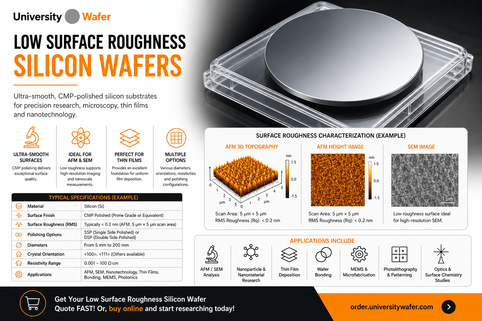
Atomic force microscopy (AFM) is commonly used to characterize silicon wafer surface morphology at very small scales. AFM measurements can provide information about surface height variations and help researchers quantify parameters such as RMS roughness.
A low-roughness substrate provides a cleaner baseline for studying nanoparticles, deposited films, surface treatments, coatings, and other nanoscale features.
SEM and Nanotechnology Research
Smooth silicon wafers are also useful as substrates for scanning electron microscopy (SEM) and nanotechnology research. Silicon provides a stable, flat platform for depositing or positioning nanoparticles, nanowires, thin films, and other microscopic structures.
Reducing unwanted surface texture can make it easier to analyze small structures and compare experimental samples under controlled conditions.
Applications for Ultra-Smooth Silicon Wafers
- Atomic force microscopy (AFM)
- Scanning electron microscopy (SEM)
- Nanoparticle and nanomaterial research
- Thin-film deposition and characterization
- Wafer bonding experiments
- MEMS and microfabrication
- Photolithography and patterning
- Optical and photonics research
- Surface chemistry studies
- Semiconductor process development
Selecting a Silicon Wafer for Your Research
The appropriate silicon wafer specification depends on more than surface roughness alone. Researchers may also need to consider crystal orientation, conductivity type, resistivity, diameter, thickness, total thickness variation (TTV), surface finish, and whether single-side or double-side polishing is required.
UniversityWafer can supply silicon substrates in a variety of specifications for surface science, nanotechnology, semiconductor processing, thin-film deposition, and other precision research applications.
Get Your Low Surface Roughness Silicon Wafer Quote FAST! Or, buy online and start researching today!
Silicon Wafer Surface Roughness and Measurement
Surface roughness is an important specification when selecting silicon wafers for precision research. At the micro- and nanoscale, small variations in surface height can influence thin-film uniformity, microscopy results, bonding quality, lithography, and the fabrication of nanoscale structures.
For applications requiring an exceptionally smooth starting surface, researchers often select prime-grade or specially polished silicon wafers produced using chemical mechanical polishing (CMP).
Common Surface Roughness Parameters
Silicon wafer surface quality can be described using several roughness parameters. The reported value should always be interpreted together with the measurement method and scan area because roughness can vary depending on the scale being evaluated.
- Ra – Average Roughness: The arithmetic average of surface-height deviations from the mean surface.
- Rq or RMS Roughness: The root-mean-square value of surface-height deviations and a common parameter in AFM surface characterization.
- Peak-to-Valley: The vertical distance between high and low points within the measured region.
How Is Silicon Surface Roughness Measured?
Different characterization techniques can be used depending on the required resolution, measurement area, and research objective.
Atomic Force Microscopy (AFM)
AFM is particularly useful for evaluating nanoscale surface topography. A small probe scans across the wafer surface and produces a three-dimensional representation of surface-height variations. Researchers can use this data to calculate parameters such as RMS roughness.
Optical Profilometry
Non-contact optical profilometry can characterize surface topography without physically touching the silicon. It is useful when researchers want to evaluate larger surface areas or avoid potential contact with sensitive surfaces.
Stylus Profilometry
A stylus profilometer physically traces the substrate surface and records vertical displacement. Profilometry is commonly used for step-height measurements, deposited-film characterization, and other surface measurements where the instrument's lateral and vertical resolution are appropriate for the feature being studied.
Surface Roughness vs. Wafer Flatness
Surface roughness and wafer flatness are not the same specification. Surface roughness describes relatively small-scale variations in surface height, while flatness parameters describe larger-scale wafer geometry.
A wafer may have an extremely smooth polished surface while still having measurable bow, warp, or total thickness variation. Researchers performing precision bonding, lithography, or metrology may therefore need to specify both surface quality and wafer geometry.
SSP vs. DSP Silicon Wafers
Low-roughness silicon substrates may be supplied as single-side polished (SSP) or double-side polished (DSP) wafers depending on the application.
SSP wafers provide a polished device or research surface on one side and are suitable for many deposition, microscopy, and fabrication processes. DSP wafers provide polished surfaces on both sides and can be advantageous for optical transmission experiments, wafer bonding, MEMS processing, backside alignment, and applications requiring high-quality surfaces on both faces.
Why Surface Quality Matters for Thin Films
When a thin film is deposited onto silicon, the underlying substrate topography can influence the morphology of the deposited layer. A smooth starting surface can therefore be important when investigating very thin coatings, interfaces, nucleation behavior, or nanoscale material properties.
Low surface roughness substrates are especially useful when researchers need to determine whether measured surface features originate from the deposited material rather than from the silicon substrate itself.
Specifications to Consider
When requesting low surface roughness silicon wafers, consider providing as much of the following information as possible:
- Required surface roughness or surface quality
- Wafer diameter
- Silicon crystal orientation, such as <100> or <111>
- P-type or N-type conductivity
- Required resistivity range
- Wafer thickness
- Single-side polished (SSP) or double-side polished (DSP)
- Total thickness variation (TTV), bow, or warp requirements
- Quantity required
Low-Roughness Silicon for Precision Research
Choosing the appropriate substrate helps establish a consistent starting surface for nanoscale characterization and fabrication. Low surface roughness silicon wafers can support research involving AFM, SEM, thin films, nanomaterials, MEMS, wafer bonding, photonics, lithography, and semiconductor process development.
UniversityWafer supplies silicon wafers in a wide range of diameters, orientations, resistivities, thicknesses, and polishing configurations to meet specialized research requirements.