
Why Use Silicon Wafers for AFM?
Silicon wafers for Atomic Force Microscopy (AFM) provide a flat, rigid, and highly polished surface that is well suited for nanoscale imaging and surface characterization. A smooth substrate helps researchers distinguish features in the sample from variations originating from the underlying surface.
This is particularly important when studying nanoparticles, thin films, two-dimensional materials, biological materials, coatings, and other structures with dimensions measured in nanometers.
Low Surface Roughness for High-Resolution AFM
Surface roughness is an important consideration when selecting an AFM substrate. If the underlying wafer has significant surface texture, that texture may interfere with measurements of small features deposited or transferred onto the surface.
Highly polished silicon provides a low-roughness background for measuring surface topography, RMS roughness, particle dimensions, step heights, film morphology, and nanoscale defects. For demanding applications, researchers should consider the specified roughness together with the AFM scan size and measurement conditions.
AFM Surface Characterization
Atomic Force Microscopy uses a very small probe mounted on a cantilever to scan across a sample surface. Interactions between the probe and sample are detected as the tip moves across the surface, allowing the instrument to construct a high-resolution representation of surface topography.
AFM can provide three-dimensional surface information without requiring the sample to be electrically conductive, making it useful for characterizing semiconductor, dielectric, polymer, biological, and nanomaterial samples deposited on silicon substrates.
Common AFM Operating Modes
Different AFM modes can be selected depending on the sample and the information required.
- Contact Mode: The probe remains in contact with the surface while scanning and can provide detailed topographic information.
- Tapping Mode: The cantilever oscillates while intermittently interacting with the sample, reducing continuous lateral contact with the surface.
- Non-Contact Mode: The probe operates above the surface and detects tip-sample interactions without continuous physical contact.
Silicon Wafers as AFM Sample Substrates
Silicon wafers can serve as a convenient platform for preparing samples before AFM analysis. Researchers may deposit, coat, transfer, or assemble materials directly onto the polished silicon surface and then examine changes in morphology and topography.
Common materials investigated on silicon substrates include:
- Nanoparticles and nanostructures
- Graphene and other 2D materials
- Metal and dielectric thin films
- Polymers and organic coatings
- Semiconductor films
- MEMS materials and structures
- Surface treatments and functional coatings
AFM for Thin-Film Research
AFM is particularly useful for studying how deposition processes affect the surface morphology of thin films. Researchers can evaluate changes in roughness, grain structure, particle formation, defects, and other surface features after deposition or processing.
Using a smooth silicon substrate provides a consistent starting surface, making it easier to compare samples produced under different deposition temperatures, pressures, times, precursor concentrations, or post-processing conditions.
Silicon Wafer Surface Preparation
Cleanliness is important for nanoscale characterization. Particles, organic residues, fingerprints, and other contaminants can appear as significant features in an AFM scan and may interfere with the interpretation of experimental results.
Researchers should select an appropriate wafer cleaning and handling procedure for their experiment and minimize unnecessary contact with the polished surface before sample preparation and AFM analysis.
Choosing Silicon Wafers for AFM Research
The ideal substrate depends on the specific AFM experiment. Important silicon wafer specifications may include:
- Surface roughness
- Wafer diameter
- Crystal orientation, such as <100> or <111>
- P-type or N-type conductivity
- Resistivity
- Wafer thickness
- Single-side polished (SSP) or double-side polished (DSP)
- Native oxide or thermal oxide requirements
- Prime, test, or research grade
AFM Applications Using Silicon Substrates
Silicon wafers can support AFM research across semiconductor processing, nanotechnology, materials science, surface chemistry, and device development. Typical applications include:
- Nanoscale surface roughness measurements
- Thin-film morphology analysis
- Nanoparticle size and distribution studies
- Graphene and 2D material characterization
- Step-height measurements
- Surface defect analysis
- MEMS research
- Coating and deposition studies
- Semiconductor surface characterization
UniversityWafer supplies silicon substrates in a wide range of diameters, orientations, resistivities, thicknesses, surface finishes, and polishing configurations for AFM and other nanoscale characterization techniques.
Get Your Silicon Wafer for AFM Research Quote FAST! Or, buy online and start researching today!
AFM Measurements on Silicon Wafer Surfaces
Atomic Force Microscopy provides nanoscale information about the topography and morphology of silicon wafer surfaces. Because AFM measures extremely small variations in surface height, substrate quality, cleanliness, scan conditions, and data-processing methods can all influence the resulting measurements.
High-quality polished silicon wafers provide a consistent reference surface for studying deposited materials, surface treatments, nanoparticles, thin films, and other nanoscale structures.
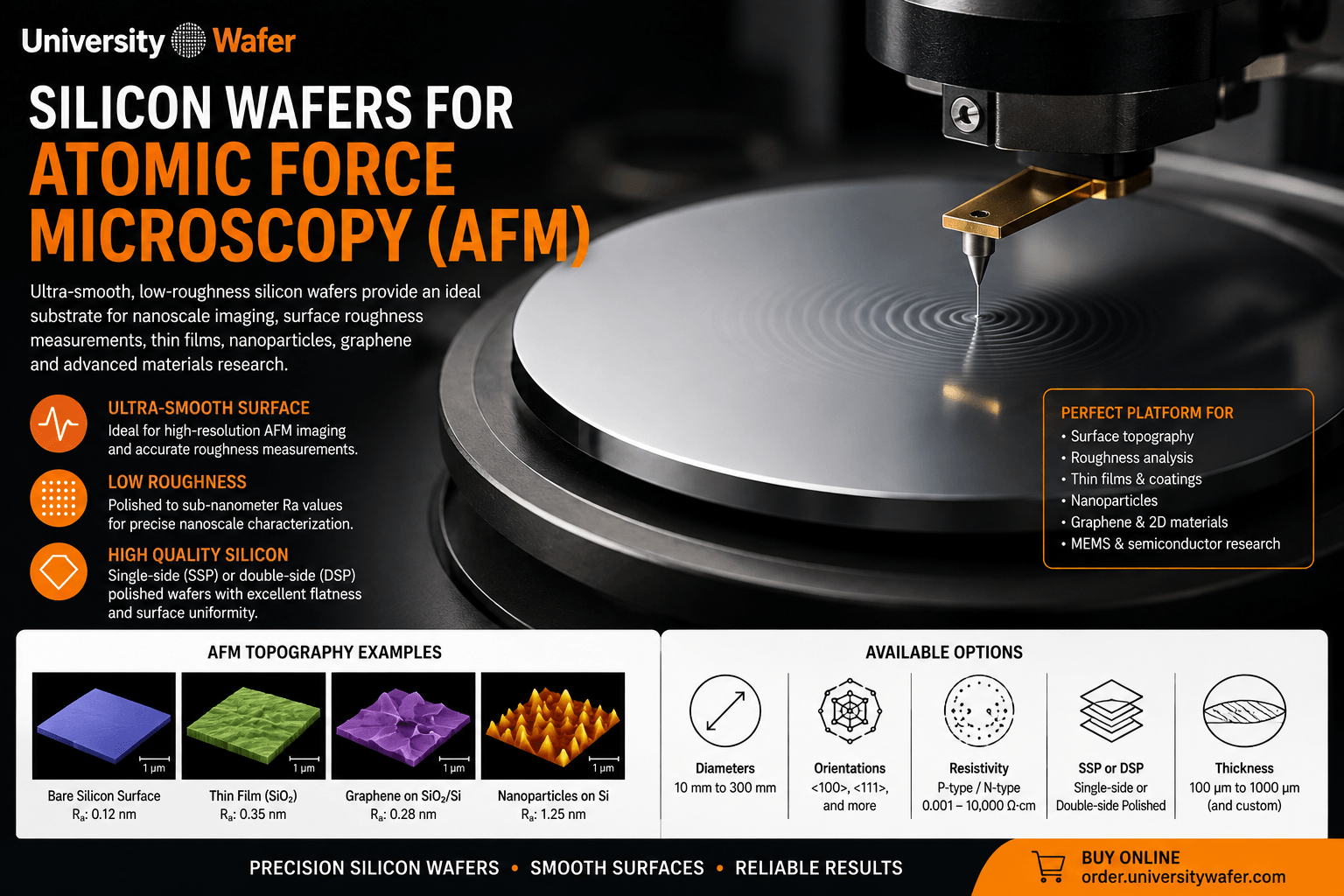
Understanding Ra and Rq Surface Roughness
AFM surface measurements are often reported using parameters such as Ra and Rq. Although both describe surface roughness, they are calculated differently.
- Ra (Average Roughness): Represents the arithmetic average of the absolute surface-height deviations from the mean surface.
- Rq (RMS Roughness): Represents the root-mean-square of surface-height deviations. Because larger deviations receive greater weighting, Rq is typically equal to or greater than Ra for the same measured area.
When comparing silicon wafer roughness values, researchers should use measurements obtained under comparable scan sizes, instrument settings, filtering methods, and environmental conditions.
Why AFM Scan Size Matters
Surface roughness is dependent on the area being evaluated. A small AFM scan may reveal nanoscale features that are difficult to observe over a much larger measurement area, while a larger scan can capture broader surface variations.
For this reason, a roughness value should ideally be reported together with the AFM scan dimensions and measurement conditions. Two measurements performed on the same silicon wafer can produce different roughness values if substantially different scan areas or analysis parameters are used.
AFM Tip and Resolution
The geometry and condition of the AFM probe can influence the apparent dimensions of nanoscale features. Tip radius, scan speed, feedback settings, vibration, contamination, and instrument calibration should be considered when performing high-resolution surface characterization.
A clean, sharp probe combined with a smooth silicon substrate can improve the ability to resolve small surface structures and produce repeatable measurements.
Native Oxide on Silicon Wafers
Silicon exposed to ambient conditions naturally develops a thin native oxide at the surface. Depending on the experiment, researchers may use the wafer with its native oxide, remove the oxide through an appropriate preparation process, or select silicon with a controlled thermal oxide layer.
Surface chemistry should therefore be considered in addition to physical roughness when silicon is used as a substrate for nanoparticles, graphene, molecular layers, coatings, or other materials.
Thermal Oxide Silicon for AFM
Silicon wafers with a controlled SiO2 layer can provide a useful substrate for AFM and nanomaterials research. Thermal oxide provides a dielectric surface and may be selected when the experiment requires a specific oxide thickness or surface chemistry.
Oxidized silicon is commonly considered for research involving thin films, nanostructures, surface functionalization, MEMS, and two-dimensional materials.
SSP vs. DSP Wafers for AFM
Both single-side polished (SSP) and double-side polished (DSP) silicon wafers can be used in AFM research.
SSP wafers provide one polished surface and are suitable for many routine surface-characterization and deposition experiments. DSP wafers provide polished surfaces on both sides and may be useful when experiments require backside processing, optical access, bonding, or high-quality surfaces on both wafer faces.
Whole Wafers or Silicon Wafer Pieces?
Many AFM experiments do not require a complete silicon wafer. Silicon wafers can be diced or cleaved into smaller pieces that fit the microscope's sample stage and reduce substrate consumption during repeated experiments.
Researchers working with wafer pieces should use clean handling procedures to avoid contaminating the polished surface during cutting, mounting, storage, and sample preparation.
AFM Sample Preparation Considerations
At nanometer-scale resolution, contamination that appears insignificant to the naked eye can become a prominent feature in an AFM image. Careful sample preparation is therefore essential.
- Handle wafers with clean wafer tweezers.
- Avoid touching the polished surface.
- Use an appropriate cleaning method for the experiment.
- Store prepared substrates in a clean environment.
- Minimize airborne particle contamination.
- Use compatible mounting materials for the AFM stage.
AFM Characterization of Thin Films
Silicon wafers provide a useful platform for comparing the surface morphology of deposited thin films. AFM can help researchers evaluate how deposition parameters influence roughness, grain formation, particle density, surface defects, and film morphology.
Measurements can be performed on the silicon substrate before deposition and repeated after processing. Comparing the two surfaces can help determine how the deposited material or treatment changed the nanoscale topography.
AFM for Nanoparticles and Nanostructures
Nanoparticles deposited onto a smooth silicon surface can be characterized using AFM to investigate properties such as particle height, distribution, aggregation, and surface coverage.
A low-roughness substrate is especially valuable when the structures being measured are only a few nanometers in height because excessive substrate texture may make small features more difficult to distinguish.
Silicon for Graphene and 2D Materials
Silicon-based substrates are widely useful for research involving graphene and other two-dimensional materials. AFM can characterize surface morphology, wrinkles, contamination, layer boundaries, and height differences after material transfer or deposition.
Researchers should select the silicon surface and oxide configuration according to the requirements of the specific 2D material and characterization method.
Specifications to Consider for AFM Substrates
When selecting a silicon wafer for atomic force microscopy, consider both the requirements of the AFM measurement and any processing that will be performed before characterization.
- Required surface roughness
- Wafer diameter or sample dimensions
- <100>, <111>, or other crystal orientation
- P-type or N-type silicon
- Resistivity range
- Wafer thickness
- SSP or DSP surface finish
- Native oxide, bare silicon, or thermal oxide
- Prime, test, or research grade
A Reliable Surface for Nanoscale Research
Selecting an appropriate silicon substrate helps establish a controlled baseline for AFM measurements. Smooth, clean, and properly specified silicon wafers can support accurate characterization of surface roughness, thin films, nanoparticles, graphene, coatings, MEMS structures, and other nanoscale materials.
UniversityWafer supplies silicon substrates with a variety of polishing options, orientations, resistivities, thicknesses, diameters, and oxide configurations for atomic force microscopy and advanced surface-science research.