
I'm putting together a grant application on advanced FSAW-type piezoelectric resonators coupled to a transmon qubit. To my points: Can you supply 4 inch or 6 inch wafers with thin films of Niobium deposited? >If so, what substrates are possible and what layer thicknesses, and do you have any characterisation of the layer morphology, properties, etc.? Is Niobium on Lithium Niobate possible? >Would it be possible to give me a quote, or an indicative non-binding ballpark price, to assist me with preparation of the grant? Thanks for taking the time to read my message. I'm really excited about this project, so if this is work you are interested in then I'd be very keen to pursue this. In any case, if you can let me know, I'd appreciate it. Best regards, have a good day.
Piezoelectric Materials We Carry
Most people have never heard of piezoelectricity, and those that have usually only know a little about it. Even scientists don't fully understand all of the implications of this phenomena.
Below are just some of the man-made Piezoelectric Substrates that we sell.
- Lithium Niobate (LiNbO3) - A manmade material for optical waveguides, mobile phones, piezoelectric sensors, optical modulators and various other linear and non-linear optical applications.
- Lithium tantalate (LiTaO3)
- Langasite (La3Ga5SiO14), a quartz-analogous crystal
- Gallium orthophosphate (GaPO4), a quartz-analogous crystal
Lithium tantalate (LiTaO3)
Get Your Quote FAST! Or, Buy Online and Start Researching Today!
What Silicon Wafers Can Be Coated with Piezoelectric Materials such as Aluminum Nitride
A scientists reqeusted a quote on the following: Any Piezoelectric thickness from 50 nm to a few microns are needed for our research. The thickness of wafer can be from 300 um to 600 um.
The piezo can be deposited on a silicon wafer <100> with thickness 300-550 um, and diameters 2 inch to 4 inch.
UniversityWafer Quoted:
2'' silicon (111) wafers coated with 25nm thickness piezoelectric materials (Aluminum Nitride),The thickness of wafer 625 um.
Contact us for pricing.
What is Piezoelectricity?
Piezoelectricity is the process of converting mechanical energy into 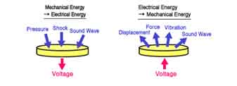 electricity. The phenomenon is useful in many areas of technology, including cell phones, diesel fuel injectors, grill igniters, vibration sensors, musical greeting cards, and clocks. It has been used for more than a century, and continues to grow in popularity. It is a candidate for our future sustainable energy supply. Along with light and thermal energy, piezoelectricity also uses human kinetic force, or motion, to convert into electrical energy.
Piezoelectric devices are commonplace, including quartz watches, voice recognition software, and scanners. These devices work by actuating materials with sound. Several examples of these devices are the following: electric lighters, tweeters, and scanning probe microscopies. It can also be used to create high voltages and electronic frequencies. Piezoelectricity is also used in many other everyday applications, including quartz watches, voice recognition, automation, and traffic control.
Piezoelectric devices are used in many applications, such as microphones and electrical cigarette lighters. The amplitude of sound waves can be converted to an electrical signal, thereby allowing it to be detected in real time. Piezoelectric crystals are also used in electric cigarette lighters to produce spark. Piezoelectric power systems are also used in larger gas and oven ranges. This technology is important in these areas, and is a growing part of our daily lives.
Top Ten Piezoelectric Materials Used by Researchers
Here are the top ten piezoelectric materials:
- Quartz
- Rochelle salt
- Lead zirconate titanate (PZT)
- Barium titanate (BaTiO3)
- Lithium niobate (LiNbO3)
- Zinc oxide (ZnO)
- Potassium niobate (KNbO3)
- Gallium orthophosphate (GaPO4)
- Lead metaniobate (PbNb2O6)
- Aluminum nitride (AlN)
Note that the ranking of these materials may vary depending on the specific application and the requirements of the piezoelectric device being used.
What Is Piezoelectric Coefficients?
Piezoelectric coefficients describe the relationship between mechanical stress or strain and electric charge or voltage in piezoelectric materials.
Types of Piezoelectric Coefficients
| Coefficient | Symbol | Description |
|---|---|---|
| Strain Coefficients | dij (m/V or C/N) | Strain induced per unit electric field, or charge generated per unit stress. |
| Stress Coefficients | eij (C/m²) | Electric field generated per unit strain. |
| Compliance Coefficients | sij (m²/N) | Elastic compliance (inverse of stiffness). |
| Permittivity | εij (F/m) | Dielectric permittivity affecting electric field response. |
| Coupling Coefficient | kij | Measures efficiency of energy conversion. |
Commonly Used Piezoelectric Coefficients
- d33: Longitudinal strain coefficient (same direction as the applied field).
- d31: Transverse strain coefficient (perpendicular to the applied field).
- e31: Piezoelectric stress coefficient (transverse).
- kt: Thickness mode coupling coefficient.
Applications
- Sensors: Convert mechanical pressure into electrical signals.
- Actuators: Convert electrical signals into mechanical motion.
- Energy Harvesting: Convert ambient vibrations into electrical power.
- Ultrasonic Devices: Used in medical imaging and industrial applications.
Substrates to Fabricate Piezoelectric Resonators
A doctor of mechanical engineering requeste the following quote:
Reference #254571 for specs and pricing.
What is Piezoelectric Materials?
Piezoelectric materials are a special class of crystals, which are electrically neutral. When mechanical pressure is applied to them, they deform and conduct an electric current. Similarly, when electrical energy is applied to them, they contract and expand. This is what we mean by net polarization. Ultimately, piezoelectric materials can be used for many applications, from generating electricity to powering electrical devices.
One of the most common uses for piezoelectric sensors is in electronic devices. They can detect pressure variations in sound waves and convert it to an electrical signal. They are also used in electric cigarette lighters, where the spark gap is filled with a tiny amount of electricity. In addition to cigarette lighters, larger gas burners and oven ranges are powered by a piezoelectric power system. The same technology is used in electric cars.
These materials have several advantages. They can be used in many applications, such as electronic drum pads and medical 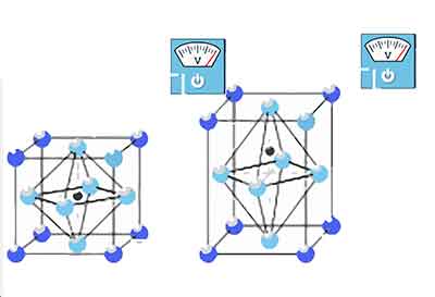 acceleromyography. Their mechanical properties are changed by external stimuli. These stimuli can be temperature, pH, or chemicals, as well as an electric field or magnetic field. This makes piezoelectric materials a versatile type of smart material. Furthermore, these materials can be categorized as intelligent functional materials because they can change their properties.
Other applications for piezoelectric materials include cell phones, diesel fuel injectors, ultrasonic transducers, vibration sensors, and musical greeting cards. They are also used in a wide variety of other applications. Despite their low price tag, the use of these materials is growing. The potential uses are endless. They are extremely versatile, and are even useful in medical devices. The next time you hear the word "electricity," consider its application.
In a piezoelectric material, stress changes its dimensions. This can cause the center of mass of the positive and negative ions to shift. The dipoles that are created throughout the material are canceled out by the other, but do not cancel each other. Instead, these dipoles are created by the stress and shift their center of mass. This is a fundamental property of piezoelectric materials.
There are many applications for piezoelectric materials. For example, gas grills and electric cigarette lighters use piezoelectric materials. The hammer strikes a piezoelectric material, which sparks, igniting the gas. The same principle applies to radios. Infrared cameras and radios are also examples of these types of devices. Besides the electric cigarette lighter, the high-tech equipment of kitchens is made with piezoelectric sensors.
For example, a piezoelectric material can convert sound energy to electrical signals, allowing them to make radio and TV signals. Piezoelectric materials are commonly used in electronic appliances such as gas grills. Moreover, they are used in various other kinds of electronics, such as telecommunications, medical imaging, and transformers. They are a great choice for applications in electronics, such as smartphones.
Other uses for piezoelectric materials are in ultrasonic flow meters and cell phones. These devices have high electrical efficiency. They can also generate sound with their low electrical resistance. The use of piezoelectric devices has expanded in many fields. The technology is widely used in automobiles, medical equipment, and other electronic appliances. For example, some printers can generate music using the vibration of a piezoelectric sensor.
The invention of piezoelectric materials began in the 1880s and is still evolving today. Researchers are working to create better and more efficient piezoelectric materials. In the past decade, there have been many applications for piezoelectric materials. For instance, some infrared cameras can use them to capture the energy of walking pedestrians. And, some other products that are made of these materials can produce a range of electromagnetic frequencies.
Currently, it is possible to create a piezoelectric material without starting with toxic materials. The only drawback of this technology is that it requires a chemical reaction that produces toxic products. However, there is a better way. Viruses can be genetically engineered and can generate a large number of identical copies of themselves in only a few hours. It can be created with the help of a human brain.
What are Some Piezoelectric Materials Research?
A piezoelectric material is a crystal that has the ability to generate electricity when compressed or vibrated. The basic principle of piezoelectricity is shown in Figure 1, and any crystal that has it is classified as pie zoelectedric crystal. When electricity is applied to the crystal, an electrical dipole appears to form due to dipoles and movement, which results in the reverse piezoelectric effect. This is called the direct pie zoe effect and is shown in Figure 2, as well as in a number of other examples. [Sources: 1, 11, 12]
A team of mechanical engineers at Virginia Tech has developed a new class of piezoelectric materials that can be used to convert motion, shock and stress into electrical energy. The technology uses existing materials and a modified 3D printer to chemically synthesize a novel piezoelectrodrical material. [Sources: 2, 14]
Piezoceramic sensors work by requiring physical force to generate energy and converting acceleration and pressure into electrical signals. The movement that is generated and the electrical energy stored in a capacitor or short-term battery are incorporated into the circuit. Since piezoelectric materials do not require physical forces to generate energy, they can function as a preloaded converter unit to convert acceleration or pressure into an electrical signal. Depending on the high dynamic load generated by the transmitters, a piezoelectronic material is able to produce a high acoustic performance, although the temperature may rise due to loss of effect. Piezolectrics materials suffer from an induced temperature rise, but they do not suffer as much as other materials, such as carbon nanotubes, because of their low heat resistance. [Sources: 3, 4, 13]
In this paper, energy generation by vibration, stress and movement is investigated using piezoelectric materials in roads. This project demonstrates for the first time the use of piezoelectric material to generate energy from road vibrations and stress movements in a roadway. [Sources: 1]
Besides piezoelectric materials, there is an additional piezoelectric term, which also refers to an electric field. Materials with the piezoelectric effect also exhibit mechanical stresses resulting from an applied electric field, and this is the basic principle of cake zoelectrodricity, as well as a number of other types of materials. When electric fields are applied to a cake material, a voltage is generated in the material and a polarity is created in it, or vice versa. [Sources: 0, 6, 8]
This voltage causes the crystalline structure to be disturbed when a pressure or voltage is applied, which then leads to an external electric field. When a piezoelectric material is exposed to mechanical stress, it takes the form of a new polarization direction of the electric dipole, which is created by pressure and voltage. PiezOELECTric materials have a material that expands over time by applying tension while the material expands further. [Sources: 1, 6, 10]
In addition to the additional strength of the base material, the flexibility of the polymer matrix provides a protective cover for the piezoelectric material and allows a variety of different shapes, such aspiezoelectric ceramic fibers, which can be better adapted to curved surfaces.piezoelectric materials can also use small voltages generated by the power of miniaturized devices to bend, stretch, bend and bend again, having the ability to stretch and stretch again and again with a small voltage and even with an electric field of up to 100 volts. piezoelectric material can also benefit from a lower stress generated by the performance of miniature miniature devices when bending, stretching, bending and bending at a voltage lower than a large voltage. [Sources: 8, 9]
Students will also learn how much (and surprisingly little) energy can be converted into piezoelectric materials using the latest technology. Students should learn more about piezoelectric materials and their applications in the field of electronics by presenting the related lessons in piezoelectric.
Nobody knows what a piezoelectric material is, but he knows what the term " piezoelectric" stands for. Based on the 6: 10, the word piezo comes from the Greek and means "the act of pressing." As this term suggests, piezoelectedric means a material that has a "piezo-electric" effect. [Sources: 1, 12]
Piezoelectricity is therefore defined as the ability to generate current through mechanical voltage or voltage. Materials that have this property fall under the category "piezoelectric." Mechanical or electrical energy can be applied to the same piezoelectedrical material and the opposite result can be achieved. When you apply an electrical signal to a material with the reverse piezo-electric effect, you can do the opposite and cause a change in the electrical properties of this material. [Sources: 5, 12]
The electrical response to mechanical stimulation is called a direct piezoelectric effect, and the mechanical response in electrical simulation is called the opposite of the piezoelectric effect. In crystalline materials, the number of electrical dipoles in a piezoelectedrical material is called a "piezoe" or "effect" and has a significant influence on the structure of this material. To summarize briefly: A "direct" piezoelectric effect refers to the change in the electrical properties of a material when it is exposed to mechanical stress. [Sources: 1, 6, 7]
Sources:
[1]: https://www.omicsonline.org/open-access/a-systematic-review-of-energy-harvesting-from-roadways-by-using-piezoelectric-materials-technology-2576-1463-1000191-99305.html
[2]: https://www.3dprintingmedia.network/3d-printed-piezoelectric-materials/
[3]: https://www.sciencedirect.com/topics/materials-science/piezoelectric-material
[4]: https://www.teachengineering.org/activities/view/uoh_piezo_lesson01_activity1
[5]: https://www.autodesk.com/products/eagle/blog/piezoelectricity/
[6]: https://www.ctscorp.com/resource-center/tutorials/piezo-basics/
[7]: https://www.comsol.com/blogs/piezoelectric-materials-crystal-orientation-poling-direction/
[8]: https://knowledge.ulprospector.com/2689/pe-piezoelectric-materials/
[9]: https://amtil.com.au/pushing-print-on-large-scale-piezoelectric-materials/
[10]: https://www.nanomotion.com/nanomotion-technology/piezoelectric-effect/
[11]: https://www.bostonpiezooptics.com/intro-to-transducer-crystals
[12]: https://www.elprocus.com/what-is-a-piezoelectric-material-working/
[14]: https://physicsworld.com/a/3d-printed-piezoelectric-materials-line-up-for-medical-applications/