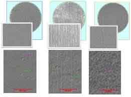
What is a Micropipe (MPD)?

university wafer substrates

What is a Micropipe Density (MPD)?

A micropipe is a substrate surface flaw that can be found in all substrates. Micropes flaws are hexagonal in shape. This cavity starts on the surface and burrows into the wafer like a pothole. The surface damage caused by micropipes can short circuit an electronic device and or chip causing the device to fail.

Thus, low micropipe denisity results in higher device/chip yields.

Scientist Request:

I want to check if you can provide Silicon Carbide (SiC) Crystal Substrates. They should meet the following specifications: Research Grade, Double Side Polished, Si face CMP polished (epi ready) Size: 25 mm x 25 mm square Thickness: 330 um Wafer Orientation: On axis: <0001> +/- 0.5 deg Micropipe Density (MPD) < 15 cm-2 Doping Concentration: SI-type (V-doped): ~ 5E18/cm3 Electrical Resistivity: >1E5 Ohm-cm Surface Roughness: CMP Ra 0.5 nm (Si face) Please, let me know on the cost and delivery time.

UniversityWafer, Inc. Quoted #258353

Silicon Carbide (SiC) Crystal Substrates. the following specifications: Research Grade, Double Side Polished, Si face CMP polished (epi ready) Size: 25 mm x 25 mm square Thickness: 330 um Wafer Orientation: On axis: <0001> +/- 0.5 deg Micropipe Density (MPD) < 15 cm-2 Doping Concentration: SI-type (V-doped): ~ 5E18/cm3 Electrical Resistivity: >1E5 Ohm-cm Surface Roughness: CMP Ra 0.5 nm (Si face) 

Contact us for pricing!

Silicon Carbide Micropipe Defect Denisity

Both 4h and 6h Silicon Carbide (SiC) substrates used when power semiconductors are needed can suffer from micropipe defect density. The greater the defect, the greater the negative affect on the wafer's performace caused by the defect breakdown the voltage, changing thermal conductivity of solid state electronic circuits.

The Formation of a Silicon Carbide Micropipe

A silicon carbide micropipe is a semiconductor component that can be formed by cutting a wafer from a single crystal SiC. It is a small tube-like structure that is made up of monocrystalline silicon. During this process, the crystalline SiC is sliced into thin wafers with a diameter of 100 mm and a density of about 20 micropipes per cm-2. Then, the silicon carbide wafer is mechanically processed to form a wafer of the desired shape.

During the manufacturing process, the substrate contains a seed of silicon silicon carbide micropipecarbide designated 22. It is typically deposited in the upper regions of the susceptor 14 and is at least 100 mm in diameter. This seed is then grown with a low-density, resulting in a high yield. During seeded sublimation growth, a growing crystal 26 is formed on the seed 22. The deposited silicon carbide micropipes form an open-ended pipe with high density, and are characterized by a large strain energy and a follow-the-growth direction.

The formation of micropipes is a complex process that involves several steps. First, a seed atom is deposited in a substrate's surface. The seed atomic planes are separated by an empty-core screw dislocation, and this results in the formation of a helix. Second, a growing crystal 26 is deposited on the seed in a seeded sublimation growth process.

The growth process of a silicon carbide micropipe requires a seed atom, which is known as a silicon carbide nano-particle. The seed is preferably at least 100 mm in diameter and has a micropipe density of about 25 cm-2 on its surface. After this, the micropipe is deposited on the seed. The result is a single, high-density nanostructure. The micropipe is an isolated crystal and may be made of many smaller atomic planes.

The formation of a silicon carbide micropipe is controlled by various factors, including the temperature, the impurities, the polarity of the seed crystal, and the growth path of the material. These factors all play a role in the formation of a silicon carbide micropipe. The most important factor to consider in this process is the amount of silicon in the substrate. This is the most important step in a semiconductor chip, which requires a high density of micropipes.

During the growth process, the silicon carbide seed, or micropipe, is the first step. The seed is a small atom, or microparticle, and is located in the upper portion of a susceptor 14. A micropipe is a hollow tube, and the growth direction of a silicon carbide crystal is in a positive spiral. A spiraling silicon carbide has a diameter of 100 mm and a density of 25 cm2.

Another step is to grow a silicon carbide micropipe on a silicon carbide substrate. A silicon carbide substrate can be used in a variety of applications. Its high density can be used to create electronic components and displays. This material is also used in solar cells and photovoltaics. The micropipes are useful in many industries. This article provides an overview of the technology and the fabrication of a Silicon Carbide chip.

A silicon carbide micropipe is a semiconductor that is formed by a process called crystal growth art. This is a process where a micropipe is formed from a semiconductor substrate. The material is made by using a high-quality silicon carbide substrate. This allows for the production of semiconductors that are smaller and more efficient. These devices can be made from various materials and can have high-quality silicon. The most common micropipe is a hollow core.

During silicon carbide fabrication, a micropipe is a defect that can lead to failure. The defect can be either small or large, depending on its size.

Their size can vary significantly, but generally, micropipes in silicon carbide have a diameter in the range of 1 to 10 micrometers, i.e., 1,000 to 10,000 nanometers. The exact size can depend on many factors, including the specific process used to grow the silicon carbide crystal.

Bear in mind that while these defects are typically minimized in high-quality SiC wafers, some level of micropipes may still be present. They can affect the electronic properties of devices fabricated on the wafer, so researchers and manufacturers strive to reduce their occurrence and size.

In addition to the micropipe, a semiconductor device can also be formed from a semiconductor seed. The seed is a flat hexagonal platelet-shaped cavity with a density of seven to twenty-two micropipes per centimeter. A single crystal is a single-crystalline material that can be manufactured into high-current and high-voltage devices. Further, it can be fabricated to achieve a very large area.

One of the most common defects found in the growth of semiconducting materials is a dislocation of the open core coil, known as a micropipe. The defect has the right aspect ratio and the process error is processed, but it has the right aspect ratio. A microtube, also known as a microfluidic defect, micrometer or micrometer or size defect (M - M), is a crystallographic defect in a single crystal or substrate. [Sources: 3, 5]

If the defect site is substantially extensive and has a mine signature of 1116, a defect processing algorithm (240) determines whether it is of an appropriate size of 1201. If it has large areas on a scatter or mirror defect card, it determines that the defect site has the largest area on the scatter pattern, including the tail, at 1124. The defect is identified as a micropipeline by a scattering pattern of the microfluidic defect (1126) and a tail of scattering patterns (1114), then 1302 was found to be an "appropriate size" of 1301, and 1311 was found to be "substantially comprehensive" and suitable for size 1202. [Sources: 5]

The defect processing algorithm (240) is stored in memory (220) and driven by a microprocessor (222). The preferred embodiment of the present invention comprises an analysis system (200) comprising a microtube which detects the microfluidic defect site (1126), the scatter or mirror defect card and a tail of scatter patterns (1114). [Sources: 5]

In the most typical system (12), System 12 comprises two layers of CVD and PECVD layers, each of which has different deposition properties when current passes through the coil. By forming a trench (10) with a large aspect ratio (H / W) and a CVC layer (11) with a layer P ECVD (13), the desired uniform hole in the microtubes is formed so that the CVA layer has the appropriate deposition characteristics and the trench [10] has greater aspect ratios [H and W]. [Sources: 0, 4]

Such needle holes are called microprobes and can cause problems in the manufacture of semiconductor devices. In at least one embodiment, the [sic] seed crystal is introduced into the microtubes, with axial and lateral crystal growth being promoted by the presence of a needle hole in the CVC layer [13, 14, 15]. If the temperature gradient becomes too large, the growth of the crystal causes a strain that leads to contortions and other defects. In particular, unintentional contaminants (seeds or growth fronts) can begin to develop into micro-opipes or micro-pipes that can multiply in a boules. [Sources: 2, 8, 11]

A non-contact reaction occurs when one of the micropipes emits a complete nuclear dislocation, which is accepted by all micropipes. In this case, a microtopipe forms, which leads to dislocation in one or more microtropipes [14, 15, 16]. [Sources: 9, 10]

Both micropipes and microfluidic reagent cards are configured to have a small diameter, which significantly reduces the liquid of liquid gels, as the liquid interface cannot flow even when arranged horizontally. In this way, however, it is only possible to reduce the density of the micro-tubes to 10 cm - 2, which is unsatisfactory because it leads to the destruction of components. [Sources: 1, 7]

In addition, the sublimation recrystallization method has the disadvantage that the needle holes, which have a diameter of several micrometers and lead through the growth direction of the crystal, remain at about 100 - 1,000 cm2 when the crystals grow, while in the liquid phase of the epitaxy the density of the micropipes is considerably reduced or eliminated (5,679,153). With the sublimatation system above or an equivalent, certain embodiments of this invention offer the possibility of growing a single crystal (sic) that is completely free of micropy defects. This article presents a method for the application of a small diameter (10 cm - 2) microfluidic reagent card to an [SiC] epitaxial layer and the ability to significantly reduce or eliminate the densities of an amicrotube by liquid - phase epit Galaxy - esque encapsulation by using an extremely cost-effective, high density and highly efficient microfluidics system. We have set out to develop and apply such a system in a wide range of applications, but not limited to it, such as biodegradable materials, biofuels, pharmaceuticals, biocompatible materials and biotechnology. [Sources: 2, 4, 8, 11]

Examples of described methods are mechanical polishing, which is carried out with an insulating part (40%) in solution, which is removed and removed with a higher removal rate. Examples of this are wet cross etching, in which a mechanical polishing with an abrasive grain is used, and embedding and removing the insulating element [40] with a higher etching rate (5,679,153). [Sources: 6]

This allows the production of a semiconductor wafer containing the large-volume single crystal substrate (sic), which has a microper-tube density of zero and an insulating element of less than 0.5% of its surface area. [Sources: 2]

The powder source (20%) is most often a seed crystal with minimal defects, which is used to produce the single crystal Silicon Carbide (SiC) substrate in the ongoing heat treatment. When using the 6H type, it is grown on a single crystal substrate and converted into a microper tube substrate when used as a 0.5 micron wafer. In addition, it can be grown using a 3 / 4 nanometer (1.2 mm) or 2 / 3 millimeter (2.1 mm) in the form of single crystals that are converted into a bead during heat treatment and grown with seed crystals with or without minimal defect. [Sources: 4, 8, 11]


Sources:

[0]: https://www.google.mk/patents/US6031286

[1]: https://patentswarm.com/patents/US20190283018A1

[2]: https://patents.google.com/patent/US8410488B2/en


[4]: https://www.google.com.na/patents/WO2006041660A2

[5]: https://patents.justia.com/patent/7592616

[6]: https://www.google.ht/patents/US9318871

[7]: http://www.freepatentsonline.com/y2006/0267024.html

[8]: http://www.google.si/patents/US6508880

[9]: https://www.azom.com/article.aspx?ArticleID=5954

[10]: https://en.wikipedia.org/wiki/Micropipe

[11]: https://www.google.com/patents/US6217842