
Alumina Wafers & Substrates in Stock
UniversityWafer supplies alumina (Al2O3) wafers and ceramic substrates for research, electronics, thin-film processing, laser experiments, sensors, and materials testing.
Alumina substrates are available in a range of sizes, thicknesses, purity levels, and surface finishes. Contact us with your specifications and quantity for current availability, pricing, and lead time.
Example High-Purity Alumina Substrate
- Material: Alumina (Al2O3)
- Purity: >99.5%
- Structure: Recrystallized alumina
- Size: 2" × 2"
- Thickness: 0.5 mm
- Typical grain size: approximately 1–10 µm
Need a different specification? Send us your required dimensions, thickness, purity, surface finish, and quantity. Pricing depends on the requested specifications and order volume.
Alumina Substrates for Laser Ablation
Alumina can be used as a durable ceramic test substrate for laser ablation, laser-material interaction, surface modification, and coating experiments.
For preliminary laser experiments, researchers may not require a tightly specified grain size, orientation, or polished surface. This can make standard-grade alumina substrates a practical option when the primary requirements are dimensions, thickness, and cost.
Example Laser Research Request
- Quantity: 5–10 pieces
- Material: Alumina (Al2O3)
- Size: approximately 2"
- Shape: Square or circular
- Thickness: 0.5 mm or greater
- Purity: Standard/typical grade acceptable
- Grain size: No special requirement
- Surface finish: No special requirement
If your experiment is flexible on purity, finish, or dimensions, mention this in your quote request. We can use those requirements to help identify an economical available option.
Alumina Wafers for Chemical Testing Devices
Alumina's electrical insulation, mechanical stability, and compatibility with deposited or patterned films make it useful as a substrate for sensors, electrodes, heaters, and experimental chemical-testing devices.
Example Research Specification
- Material: Alumina (Al2O3)
- Diameter: 100 mm
- Thickness: 0.800 mm
- Polish: Single-side polished (SSP)
- Flats: None required
- Reference: #265621
These specifications are an example of a previous research requirement. Contact UniversityWafer for current availability, pricing, alternative specifications, and lead time.
Get Your Alumina Wafer Quote FAST! Tell us your required Al2O3 purity, size, thickness, surface finish, and quantity. Or, Buy Wafers Online and Start Researching Today!
What Are Alumina Wafers?
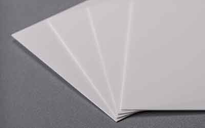 Alumina wafers, also called alumina substrates or
aluminum oxide (Al2O3) ceramic substrates,
are rigid ceramic plates used as electrically insulating and mechanically stable
platforms for electronic, thin-film, sensor, optical, and research applications.
Alumina combines good mechanical strength, electrical insulation, thermal stability,
and useful thermal conductivity in a comparatively economical ceramic material.
Alumina wafers, also called alumina substrates or
aluminum oxide (Al2O3) ceramic substrates,
are rigid ceramic plates used as electrically insulating and mechanically stable
platforms for electronic, thin-film, sensor, optical, and research applications.
Alumina combines good mechanical strength, electrical insulation, thermal stability,
and useful thermal conductivity in a comparatively economical ceramic material.
Alumina substrates can be manufactured in circular, square, or rectangular formats and in a range of thicknesses, surface finishes, and purity grades. High-purity material is especially useful when contamination control, surface quality, dielectric performance, or demanding thin-film processing is important.
Although alumina and sapphire have the same basic chemical formula, Al2O3, they are not the same substrate. Conventional alumina ceramic is polycrystalline, while sapphire is single-crystal Al2O3. Their surface, optical, mechanical, and processing characteristics therefore differ.
Why Use Alumina as a Substrate?
Alumina is widely used in electronic substrate technology because it provides a useful balance of electrical, thermal, mechanical, and manufacturing properties. Dense alumina has high electrical resistivity and dielectric strength, allowing it to electrically isolate conductive traces or devices while providing a strong supporting structure.
Its thermal conductivity is substantially higher than that of many polymeric electrical insulators, helping move heat away from electronic components while maintaining electrical isolation. Alumina also remains dimensionally stable across a broad temperature range and offers good resistance to many chemicals encountered in laboratory and industrial environments.
Thin-Film and Thick-Film Alumina Substrates
Alumina is commonly used as a base material for both thin-film and thick-film metallization. For thin-film processing, surface smoothness, flatness, porosity, and defect density are especially important because the substrate surface can directly affect fine-line pattern definition and film continuity.
Polished high-purity alumina can support deposited metal and dielectric films used in microelectronic circuits, sensors, resistors, and other patterned devices. Thick-film processes can use conductive, resistive, and dielectric pastes that are printed onto the ceramic and subsequently fired to create functional circuitry.
Alumina Wafer Applications
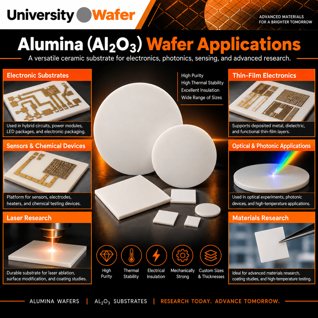
Alumina substrates are used across research and industrial applications where electrical insulation, structural stability, and elevated-temperature performance are required. Typical uses include hybrid integrated circuits, thin-film circuits, thick-film circuits, sensor platforms, LED packages, thermal print heads, power modules, electronic packaging, and experimental device fabrication.
Thin-Film Electronics and Microfabrication
Smooth alumina surfaces can be used for depositing metals, dielectric layers, resistive films, and other functional materials. Researchers can pattern these layers using common microfabrication techniques to investigate sensors, microelectronic structures, electrodes, and experimental thin-film devices.
Power Electronics and Electrical Insulation
Because alumina is electrically insulating while still capable of transferring heat, it is commonly used as a ceramic circuit carrier and insulating support in electronic assemblies. Alumina substrates can support metallized structures while electrically separating conductive components from surrounding hardware.
Laser and Materials Research
Alumina substrates can also serve as durable test coupons for laser ablation, surface modification, coating adhesion, materials characterization, and high-temperature experiments. Researchers may select substrate thickness, purity, surface finish, and dimensions according to the laser wavelength, deposited material, or experimental configuration.
Sensors and Chemical Testing Devices
Alumina's electrical insulation, mechanical rigidity, thermal stability, and compatibility with metallization make it useful as a platform for experimental sensors and chemical-testing devices. Conductive traces, electrodes, heaters, or sensing films can be deposited or patterned on the ceramic surface depending on the device design.
Alumina Purity and Surface Finish
Alumina ceramics are commercially available in several purity grades, commonly including approximately 96% through 99.6% Al2O3. Increasing purity can change properties such as dielectric behavior, surface characteristics, thermal performance, and suitability for demanding thin-film processes. The best grade depends on the application rather than purity alone.
Surface condition is also important. As-fired alumina may be sufficient for many mechanical, insulating, or thick-film applications, while polished surfaces are preferred when low roughness, fine patterning, uniform thin-film deposition, or precise interfaces are required.
Choosing an Alumina Substrate
When requesting an alumina wafer or substrate, consider the diameter or lateral dimensions, thickness, Al2O3 purity, surface finish, flatness, quantity, and intended process. Requirements for thin-film deposition may be very different from those for laser testing, power electronics, or general laboratory use.
UniversityWafer can supply alumina wafers and Al2O3 ceramic substrates for research and development in a variety of dimensions and specifications. Contact us with your required size, thickness, purity, surface finish, and quantity so we can help identify an appropriate substrate for your application.