ADVANCED CRYSTAL SCIENCES LPCVD SYSTEM
ADVANCED CRYSTAL SCIENCES LPCVD SYSTEM
Manufacturer: Advanced Crystal Sciences
2 tube lpcvd system bpsg system boron, phosphoros, silane, glass for low temperature glass reflow includes vacuum pumps
Get Your Quote FAST!
Advanced Crystal Sciences Lpcvd System
Key technologies for experimental nanotechnology, including laboratory safety, are covered by the Science Office of the National Science Foundation (NSF) of the US Department of Energy. [Sources: 6, 7]
Students of nanosciences are introduced to technical cell systems, and suitable project topics are tripod polishing, microfluidic devices, nanoscale nanostructures and microelectrochemical systems. [Sources: 7] 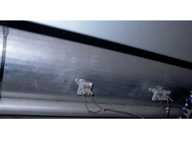
UniversityWafer, Inc. and partners have thousands of machines in stock. Please let us know the equipment that you're interested in.
If would would like to see an emailed video of the ADVANCED CRYSTAL SCIENCES LPCVD SYSTEM you have purchased in operation prior to shipment, please let us know. Please note: We may need a deposit prior to sending a video of the ADVANCED CRYSTAL SCIENCES LPCVD SYSTEM to cover techncian costs.
About Furnaces
In a controlled environment, the fast-growing Ori of graphene crystals overwhelms the others and is selected as a single crystal that matches the Ori of the substrate, and overloads each other. Large crystals form easily and discreet smaller crystals have a regular triangular morphology that forms the figure-bearer. With the growth of single crystals, it is also recognised that the number of nanoscale nanostructures in a graphene crystal is rapidly increasing. Depending on the size and shape of the graph and its Ori in the crystal structure, two possibilities for the growth of the crystals can be investigated: the formation of large and small crystals in different Oris. [Sources: 0, 2, 8]
The first successful Ori - controlled synthesis of a single graphene crystal - was realized with Cu-111 on behalf of the research team of the Institute of Materials Science and Engineering (IME) at the University of California, Berkeley. [Sources: 4]
For example, by introducing oxygen into the Cu surface, an inch of Cu-001 was induced and a 12 cm Cu-111 surface was achieved by activating hydrogen 11. To evaluate the potential of the new method for cultivating other TMDs (crystals), we have tried to synthesize MoSe-2 and WS-2 crystals using a similar strategy. We found that by controlling the growth process using the two-stage CVD method, the nucleation density of Mo (2) was significantly reduced and larger crystals were also produced. [Sources: 0, 4]
MoSe-2 crystals were characterized using Raman spectra and the maps presented in this paper using a selected scanning electron microscope. In addition, the researchers at the MQ Photonics Research Centre have developed a diamond Ramans laser, which is the most powerful single crystal CVD laser in the world. The optical single crystals of the CVC diamond can be used to develop state-of-the-art laser technology, opening up new opportunities in many fields, including optical and optical microscopy, photonics, nanotechnology and nanophotonics. [Sources: 0, 1, 5]
Diamond CVD is the use of the different diamond sources, integers in different diamonds and source sections, which, due to their thermodynamics and metastability, offer the possibility of synthesizing composites based on the diamond even under soft conditions. The main advantage of using single crystal CVC diamond (MoSe-2) in this example is that the overall reflection of an ATR crystal is attenuated. This is due to its high thermal conductivity, which means that IR samples with a high resolution of less than 0.5 micrometers per square centimeter are possible without affecting the ATr crystal. [Sources: 2, 5]
One of the problems with batch furnace systems is that they cannot simultaneously absorb nano-crystal films in an environment of high temperature and pressure. The LPCVD Chamber 100 provides the separation environment, but there is no precise control of temperature or pressure. We have developed a process in which students in an academic district have the opportunity to produce a complete CMOS IC wafer using the SNSF system and to learn practical skills safely through the process and laboratory techniques. This enables the development of high-quality, cost-effective, high-performance and high-quality materials. [Sources: 6, 9]
At low temperatures, glass containing boron, phosphorus and boron-sophosphosilicate glass (BPSG) is subject to a viscous flow, and air stability can be difficult to achieve. At 850 degrees Celsius, which is a high temperature for a glass containing 5% of its weight of components, the crystal is etched with standard reactive plasmas to model the oxides. The flow may also precipitate crystals of BPO-4 when cooling, but these crystals will cause circuit errors during the manufacture of integrated circuits. [Sources: 3]
In one embodiment, nano-crystal silicon films may be discontinuous and form by bonding capacitors and electrodes, while in another embodiment, doped silicon wafers (502) are formed by dielectric (504) layers forming an intermediate layer of silicon (503, 502, 503). In a single - wafer chamber, undoped or dope - nanocrystal - silicon formation of BPO-4 and boron - sophosphosilicate glass can be achieved. [Sources: 9]
The precursor gas is fed into the reaction chamber (90) and then into a high-pressure, low-pressure chamber with high pressure and high temperature (100). [Sources: 9]
Sources:
[0]: https://onlinelibrary.wiley.com/doi/abs/10.1002/advs.201600033
[1]: https://www.mdpi.com/2073-4352/10/4/308/htm
[2]: https://www.scielo.br/scielo.php?script=sci_arttext&pid=S0103-97332000000300002
[3]: https://en.wikipedia.org/wiki/Chemical_vapor_deposition
[4]: https://www.nature.com/articles/srep45358
[6]: http://tvonline.pe/4llg9l/cmos-fabrication.html
[7]: https://sunypoly.edu/academics/majors-and-programs/ms-nanoscale-science/courses
[8]: https://www.energy.gov/science/bes/articles/scaling-single-crystal-graphene
[9]: https://www.google.si/patents/US20070287271