
Single Crystal Quartz Wafers for Nanochannel Fabrication and Research
A Ph.D. candidate contacted UniversityWafer, Inc. looking for single crystal quartz wafers and Borofloat 33 glass substrates for advanced microfabrication research. Their project required materials suitable for both anodic bonding with silicon wafers and nanochannel fabrication.
The researcher requested:
- 50 Borofloat 33 glass wafers (ID #517)
- 25 single crystal quartz wafers (ID #1210)
Borofloat 33 Glass for Silicon Anodic Bonding
Borofloat 33 glass wafers are frequently used for MEMS devices, microfluidics, and wafer-level packaging because their thermal expansion closely matches silicon. This makes them ideal for anodic bonding applications and hermetic sealing processes.
Single Crystal Quartz for Nanochannel Fabrication
The researcher planned to use single crystal quartz substrates to fabricate nanochannels using sacrificial layer etching techniques. Quartz substrates are popular for nanotechnology, biosensors, optical devices, and microfluidic applications because of their excellent optical transparency, chemical resistance, and thermal stability.
Our engineering team confirmed that both materials were excellent choices for the application and provided specifications and pricing under Reference #209714.
Get Your Single Crystal Quartz Quote FAST!
Or Buy Online and Start Researching Today!
Seeded and Seedless Single Crystal Quartz Wafers in Stock
UniversityWafer, Inc. supplies seeded and seedless single crystal quartz wafers in a variety of crystal cuts, diameters, thicknesses, and polish configurations. We offer both single-side polished (SSP) and double-side polished (DSP) quartz substrates for optical, piezoelectric, MEMS, sensor, and semiconductor research.
Please let us know your desired diameter, orientation, thickness, polish, and quantity so we can provide a fast quote.
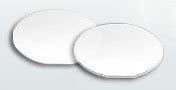
Single Crystal Quartz Wafers and Substrates
UniversityWafer, Inc. supplies single crystal quartz wafers and quartz substrates for research, optics, sensors, resonators, frequency-control devices, and classroom experiments. Quartz is valued for its excellent thermal stability, optical transmission, piezoelectric properties, and strong mechanical performance.
We stock a selection of single crystal quartz wafers in common orientations and cuts. If your project requires fused silica wafers instead of crystalline quartz, please contact us and we can help you select the correct material.
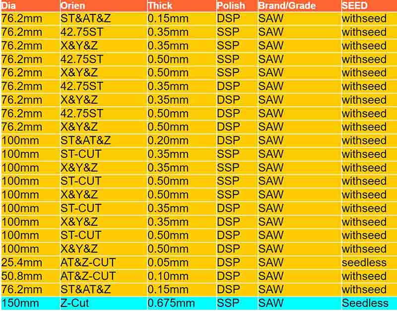
Common Quartz Wafer Cuts
Single crystal quartz can be supplied in different crystal cuts, including AT-cut, ST-cut, X-cut, Y-cut, and Z-cut quartz. The best cut depends on the device design, crystal orientation, frequency behavior, optical axis, and temperature-stability requirements.
AT-Cut Quartz
AT-cut quartz wafers are commonly used for resonators, oscillators, frequency-control devices, filters, and timing applications. This cut is popular because it offers strong frequency stability and good performance across changing temperature conditions.
ST-Cut Quartz
ST-cut quartz substrates are often selected for surface acoustic wave devices, sensors, and high-frequency research. ST-cut quartz provides useful piezoelectric behavior and is used when acoustic wave propagation and crystal orientation are important to the device.
X-Cut and Y-Cut Quartz
X-cut quartz and Y-cut quartz are used in optical, electrical, and piezoelectric applications where the direction of the crystal axis affects performance. These cuts may be used for resonators, sensors, optical components, and experimental device fabrication.
Z-Cut Quartz
Z-cut quartz wafers are useful when alignment with the optical axis is required. Researchers may choose Z-cut quartz for optical components, infrared research, spectroscopy, and experiments that depend on quartz crystal orientation.
Quartz Wafer Applications
Single crystal quartz wafers are used in many research and production areas, including:
- Quartz resonators and oscillators
- Frequency-control and timing devices
- Surface acoustic wave devices
- Optical windows and precision optical components
- Infrared sensors and spectroscopy research
- Microwave circuits and telecommunications research
- Biosensors and laboratory experiments
- Thin-film deposition and device prototyping
Related Pages
- Borofloat 33 and Pyrex Glass Wafers
- MEMS Substrates and Applications
- Surface Acoustic Wave (SAW) Devices
- Lithium Niobate (LiNbO3) Wafers
- Silicon Wafers
- Biosensor Applications
- Optical Windows and Optical Substrates
- Piezoelectric Materials and Devices
- RF and Microwave Applications
- Thin Film Deposition and Coatings