
Glass Wafers for Research & Device Fabrication
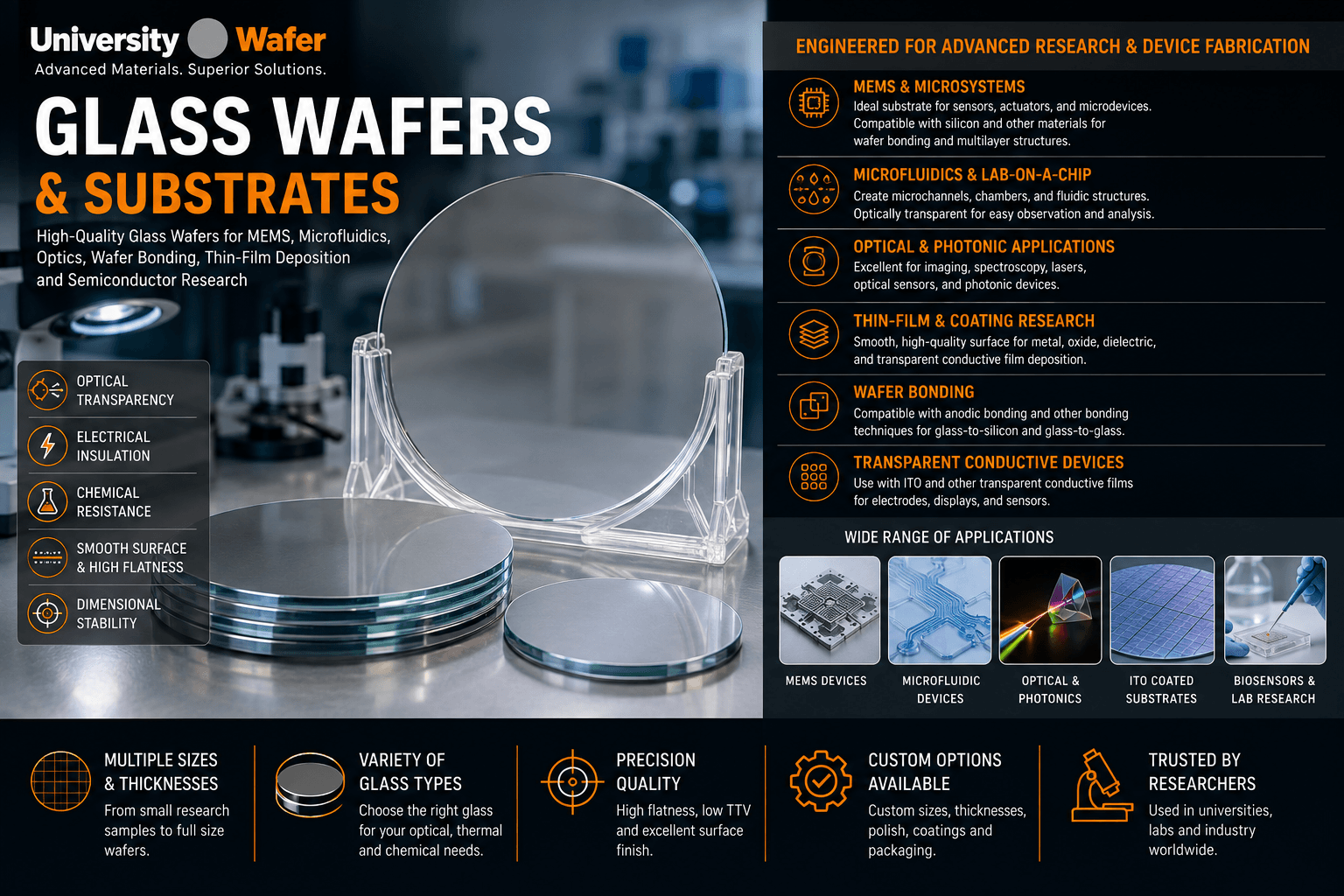
Glass wafers are widely used as substrates in semiconductor processing, MEMS fabrication, microfluidics, optics, sensors, and thin-film research. Their combination of optical transparency, electrical insulation, chemical resistance, and surface quality makes glass an excellent alternative to conventional semiconductor substrates for many specialized applications.
UniversityWafer supplies glass wafers and substrates for universities, laboratories, semiconductor developers, and industrial R&D. Different glass compositions, wafer diameters, thicknesses, surface finishes, and processing options can be selected depending on the requirements of the experiment or device.
Why Use Glass as a Wafer Substrate?
Glass offers several properties that are valuable for microfabrication and research. Unlike conductive semiconductor materials, glass is electrically insulating while remaining compatible with many deposition, patterning, bonding, and etching processes.
- Optical transparency: Useful for imaging, optical sensing, microscopy, and devices requiring transmission through the substrate.
- Electrical insulation: Helps electrically isolate components and structures in MEMS and electronic devices.
- Chemical resistance: Suitable glass compositions can withstand many chemicals encountered during laboratory and fabrication processes.
- Smooth surfaces: Polished glass wafers provide surfaces suitable for thin-film deposition, lithography, bonding, and device fabrication.
- Dimensional stability: Properly selected glass substrates provide stable platforms for precision research and microfabrication.
Glass Wafers for MEMS
MEMS glass substrates can be used to fabricate sensors, actuators, microstructures, and other microsystems. Glass is especially valuable when a device requires electrical isolation or optical access through the substrate.
Glass may also be bonded to silicon wafers to create multilayer structures. Silicon-to-glass bonding is commonly investigated for MEMS packaging, sensor fabrication, microfluidic devices, and other microsystem applications.
Microfluidic Glass Substrates
Glass is an important substrate material for microfluidic and lab-on-a-chip research. Microchannels and other small structures can be fabricated into or onto glass surfaces to control extremely small quantities of liquids and gases.
The transparency of glass also allows researchers to observe fluids, particles, cells, and chemical reactions through the substrate using microscopes, cameras, and optical detection systems.
Optical & Photonic Applications
Optical-grade glass substrates are useful for experiments involving light transmission, imaging, lasers, spectroscopy, sensors, and photonic structures. Depending on the required wavelength range and thermal properties, researchers may also consider specialized materials such as fused silica wafers or quartz substrates.
Thin-Film Deposition on Glass
Polished glass wafers provide a stable surface for depositing metals, oxides, transparent conductive films, dielectric layers, and other research materials. Common deposition and fabrication processes can include sputtering, evaporation, chemical vapor deposition, photolithography, and surface coating.
Researchers developing transparent conductive structures may also use ITO-coated wafers for displays, sensors, electrodes, photovoltaic experiments, and optoelectronic devices.
Selecting a Glass Wafer
The appropriate glass substrate depends on the fabrication process and final application. Important specifications can include glass composition, wafer diameter, thickness, surface roughness, flatness, thermal expansion, optical transmission, and polishing requirements.
Choosing a glass with a compatible coefficient of thermal expansion can be especially important when the substrate will be bonded to silicon or another material that experiences heating during fabrication.
Get Your Glass Wafer Quote FAST! Or, Buy Wafers Online and Start Researching Today!
Glass Wafer Applications
Glass wafers and substrates are used across semiconductor manufacturing, biotechnology, optics, MEMS, microfluidics, and advanced materials research. Their transparency and electrical insulation make them especially useful for devices where researchers need optical access while maintaining electrical isolation between components.
MEMS Sensors & Devices
Glass substrates can serve as structural, packaging, or supporting layers in MEMS devices. Applications include pressure sensors, accelerometers, micro-actuators, optical MEMS, and other microsystems. Glass can also be combined with silicon wafers to create more complex device structures.
Microfluidics & Lab-on-a-Chip Devices
Microfluidic glass wafers are useful for fabricating channels, chambers, reservoirs, and other microscopic fluid-handling structures. Because many types of glass are optically transparent, researchers can observe processes occurring inside a microfluidic device using microscopy and optical detection techniques.
Glass-based microfluidic platforms are researched for applications including:
- Lab-on-a-chip systems
- Biomedical sensors
- Chemical analysis
- Cell and particle research
- Microreactors
- Diagnostic device development
Wafer Bonding
Glass-to-silicon wafer bonding can be used to create sealed cavities, protective covers, microfluidic channels, and multilayer MEMS structures. Anodic bonding is one technique used with suitable glass compositions to form strong bonds between glass and silicon.
The thermal expansion characteristics of the selected glass should be considered when designing bonded structures, particularly when processing involves elevated temperatures.
Optical Sensors & Photonic Devices
Transparent glass wafers provide a useful platform for optical sensors, imaging devices, photonic structures, spectroscopy experiments, and laser research. Light can pass through the substrate, allowing glass to function as both a mechanical support and an optical component.
For applications requiring specialized optical or thermal properties, materials such as fused silica wafers, BK7 glass, and BOROFLOAT® 33 glass may also be considered.
Transparent Conductive Devices
Glass substrates can be coated with transparent conductive materials such as indium tin oxide (ITO). These structures are commonly researched for transparent electrodes, sensors, displays, photovoltaic devices, and optoelectronics.
Researchers requiring a conductive transparent surface can explore ITO wafers and substrates for these applications.
Thin-Film & Coating Research
Polished glass provides a smooth substrate for depositing and characterizing metal, dielectric, semiconductor, and optical thin films. Depending on the research process, coatings may be deposited using sputtering, evaporation, chemical vapor deposition, or other thin-film techniques.
Common Glass Wafer Research Areas
- MEMS and microsystem fabrication
- Microfluidics and lab-on-a-chip devices
- Optical and photonic research
- Semiconductor processing
- Wafer bonding experiments
- Thin-film deposition
- Transparent electrodes
- Sensor development
- Biomedical research devices
- University and laboratory R&D
Custom Glass Wafer Requirements
Glass wafer requirements can vary considerably between applications. Researchers may need specific diameters, thicknesses, surface finishes, optical properties, thermal characteristics, or glass compositions. Selecting the appropriate substrate helps improve compatibility with subsequent lithography, deposition, etching, bonding, and characterization processes.