
ITO Wafers for Research
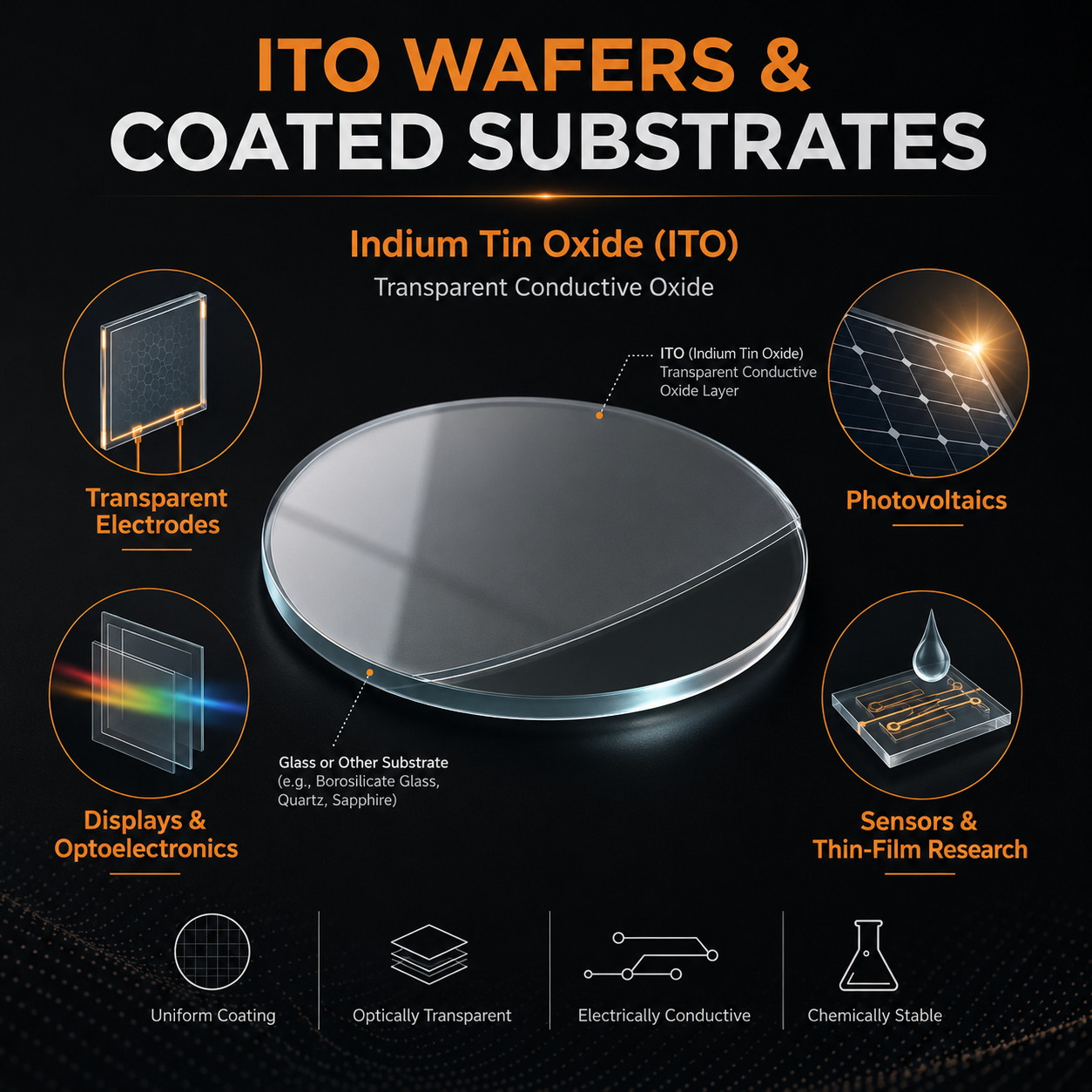
Indium Tin Oxide (ITO) wafers and coated substrates combine optical transparency with electrical conductivity. ITO is a widely used transparent conductive oxide (TCO) for research involving photovoltaics, optoelectronics, sensors, displays, thin films, and advanced electronic devices.
What Is Indium Tin Oxide?
Indium Tin Oxide is a semiconductor material composed primarily of indium oxide (In2O3) with tin oxide (SnO2). When deposited as a thin film, ITO can provide the useful combination of visible-light transparency and electrical conductivity required for transparent electrode applications.
ITO as a Transparent Conductive Oxide
Transparent conductive oxides are important when a device requires both electrical conduction and the transmission of light. ITO coatings can function as transparent electrodes, allowing researchers to electrically contact a device while maintaining optical access to the underlying layers.
ITO for Photovoltaic Research
ITO-coated substrates are widely studied in solar cells and photovoltaic devices. The conductive transparent layer can be used as an electrode while allowing light to reach the photoactive material. Researchers can investigate film thickness, surface properties, optical transmission, sheet resistance, and interfaces between ITO and other device layers.
Optoelectronic and Display Applications
ITO is also used in research involving LEDs, OLEDs, photodetectors, touch-sensitive devices, and display technologies. Its combination of electrical and optical properties makes it a versatile material for experimental devices that interact with both light and electrical signals.
Common ITO Research Applications
- Transparent conductive electrodes
- Solar cells and photovoltaic research
- LED and OLED device development
- Optoelectronic devices
- Photodetectors and optical sensors
- Touchscreen and display research
- Thin-film characterization
- Electrochemical and biosensor research
Selecting an ITO-Coated Substrate
Important specifications can include substrate material, dimensions, ITO film thickness, sheet resistance, optical transmission, surface finish, and coating configuration. The appropriate specifications depend on the electrical, optical, deposition, lithography, or device-fabrication requirements of the experiment.
ITO Substrates for Thin-Film Research
ITO-coated wafers and substrates can provide a conductive base for depositing additional semiconductor, dielectric, organic, or functional thin films. This makes them useful for studying material interfaces, electrical contacts, optical properties, and prototype device structures.
Need ITO Wafers or Coated Substrates?
Tell us your required substrate material, dimensions, ITO coating specifications, sheet resistance, quantity, and intended application. UniversityWafer can help identify an ITO-coated substrate suitable for your research.
Get Your ITO Wafer Quote FAST! Or Buy Online and Start Researching Today!
Why Use ITO-Coated Wafers?
Indium Tin Oxide (ITO) is one of the most widely used transparent conductive oxides (TCOs). An ITO coating can transmit visible light while providing electrical conductivity, making ITO-coated substrates useful for devices that require both optical access and electrical contact.
ITO for Transparent Electrodes
ITO thin films are commonly used as transparent electrodes in optoelectronic devices. Researchers can use ITO-coated substrates to investigate electrical contacts, charge transport, optical transmission, and interfaces between conductive and functional material layers.
ITO in Solar Cells and Photovoltaics
In photovoltaic research, ITO can serve as a transparent conductive electrode that allows light to reach the active layers of a solar cell while providing an electrical pathway for collecting charge carriers. ITO substrates are useful for thin-film, organic, perovskite, and other experimental photovoltaic structures.
ITO for Displays, LEDs and OLEDs
The combination of conductivity and transparency makes ITO valuable for research involving displays, LEDs, OLEDs, and other optoelectronic devices. Its transparent electrode function enables electrical operation without substantially blocking the device's optical path.
ITO for Sensors and Photodetectors
ITO-coated substrates can also support sensor and photodetector research. Researchers may deposit additional semiconductor, dielectric, biological, or functional materials onto the ITO surface to create and characterize experimental device structures.
Important ITO Film Properties
When selecting an ITO-coated substrate, researchers should consider the relationship between sheet resistance, optical transmission, film thickness, surface quality, and substrate material. These characteristics can influence both the electrical and optical performance of the finished device.
Common ITO Wafer Applications
- Transparent conductive electrodes
- Solar cells and photovoltaic devices
- LED and OLED research
- Touchscreen and display development
- Photodetectors and optical sensors
- Electrochemical and biosensors
- Thin-film deposition research
- Optoelectronic device fabrication
ITO Thin-Film Processing
ITO-coated substrates can be incorporated into processes involving photolithography, etching, thin-film deposition, patterning, and device fabrication. Additional functional layers can be deposited over the conductive ITO surface for experimental multilayer structures.
Selecting the Right ITO Substrate
Important specifications can include substrate material, substrate dimensions, ITO thickness, sheet resistance, optical transmission, surface finish, and coating configuration. Selecting these parameters according to the intended experiment can help researchers obtain a substrate appropriate for their electrical and optical needs.
ITO Wafers for Advanced R&D
UniversityWafer supplies ITO-coated wafers and substrates for universities, laboratories, prototype development, and advanced research. These materials can support photovoltaic, optoelectronic, sensor, display, and thin-film experiments.