I need 150mm P(100) 650um Double Side Polished Silicon Wafers that Have a One Micron Total Thickness Variation (TTV). They will be used as mirrors for optical sensor fabrication.
Substrates Used to Fabricate Optical Sensors
Ultra-Flat Silicon Wafer Surface to Fabricate Mirrors for Optical Sensors
A PhD student requested the following quote for their optical sensor research.
Reference #117003 for specs and pricing.
Get Your FAST! Or, Buy Online and Start Researching Today!
Optical Sensor Reflector
A Reserch Development and Design (RDD) engineer requested a quote for the following:
I am working on an optical sensor development project. One of the components in this sensor is a piece of silicon which will be used as a reflector. The silicon is 750 micron diameter x 16 micron thickness. It will be attached to a fused silica rod.
Do you sell silicon this thin or in this diameter? What is the thinnest silicon that is available; I assume that I will be able to polish it to the desired thickness after it is bonded. Is this diameter available? If not, what is the closest diameter available?
Reference #128860 for specs and pricing.
What is a RDD Engineer?
An RDD engineer, or Research, Development, and Design engineer, is a professional responsible for creating and improving products through research, development, and design processes. Their role typically involves:
- Research: Investigating new technologies, materials, and methods to innovate and improve product performance and efficiency.
- Development: Translating research findings into practical applications, creating prototypes, and testing them to ensure they meet required standards and specifications.
- Design: Crafting detailed plans and specifications for products, ensuring they are functional, aesthetically pleasing, and manufacturable.
RDD engineers work across various industries, including electronics, automotive, aerospace, and consumer goods, contributing to the advancement of technology and product innovation.
How Is Silicon Used To Fabricate Mirrors For Optical Sensors?
Silicon is widely used in the fabrication of mirrors for optical sensors due to its advantageous properties, including high reflectivity in the infrared spectrum, good thermal conductivity, and compatibility with semiconductor manufacturing processes. Here's an overview of how silicon is used in this context:
-
Substrate Material:
- High Purity Silicon: High-purity silicon wafers, similar to those used in
 the semiconductor industry, serve as the base substrate for the mirror. The flatness and smoothness of these wafers are crucial for creating high-quality mirrors.
- High Purity Silicon: High-purity silicon wafers, similar to those used in
-
Surface Preparation:
- Polishing: The silicon wafer surface is polished to achieve a high degree of smoothness, which is essential for optical applications. This step reduces surface roughness, minimizing scattering and maximizing reflectivity.
-
Coating:
- Reflective Coating: While silicon itself has good reflectivity, particularly in the infrared range, additional coatings are often applied to enhance reflectivity across a broader spectrum or to provide specific optical properties. Common coatings include:
- Metallic Coatings: Metals such as aluminum, silver, or gold are deposited onto the silicon surface to improve reflectivity. These coatings are typically applied using physical vapor deposition (PVD) techniques like sputtering or evaporation.
- Dielectric Coatings: Multilayer dielectric coatings can be applied to create highly reflective surfaces through constructive interference. These coatings are made from alternating layers of materials with different refractive indices, such as silicon dioxide (SiO2) and titanium dioxide (TiO2).
- Reflective Coating: While silicon itself has good reflectivity, particularly in the infrared range, additional coatings are often applied to enhance reflectivity across a broader spectrum or to provide specific optical properties. Common coatings include:
-
Patterning:
- Microfabrication Techniques: Silicon mirrors used in optical sensors often require precise patterning to create microstructures or integrate with other optical components. Techniques such as photolithography and etching are employed to define these patterns.
-
Integration:
- Assembly: Silicon mirrors are often integrated with other components of the optical sensor system, such as detectors and lenses. Silicon’s compatibility with semiconductor processes allows for seamless integration with electronic and photonic devices.
-
Protective Coatings:
- Anti-Reflective Coatings: To minimize unwanted reflections and enhance the performance of the optical system, anti-reflective coatings may be applied to the back surface of the silicon mirror.
- Environmental Protection: Protective coatings can also be added to protect the mirror from environmental factors such as oxidation, moisture, and mechanical wear.
Advantages of Silicon Mirrors in Optical Sensors:
- High Reflectivity in IR: Silicon has excellent reflectivity in the infrared spectrum, making it ideal for sensors that operate in this range.
- Thermal Stability: Silicon's good thermal conductivity ensures that mirrors can handle high-power applications and maintain stability under varying thermal conditions.
- Compatibility: Silicon's compatibility with standard semiconductor processing techniques allows for the integration of optical and electronic functions on the same chip.
Applications:
- Infrared Sensors: Used in thermal imaging, remote sensing, and spectroscopy.
- LIDAR Systems: Utilized in automotive and industrial LIDAR systems for distance measurement and 3D mapping.
- Fiber Optic Communication: Employed in systems where precise optical alignment and high reflectivity are critical.
In summary, silicon is a crucial material in the fabrication of mirrors for optical sensors due to its reflectivity, thermal properties, and compatibility with semiconductor manufacturing, enabling high-performance optical devices in various applications.
What Is An Optical Flow Sensor?
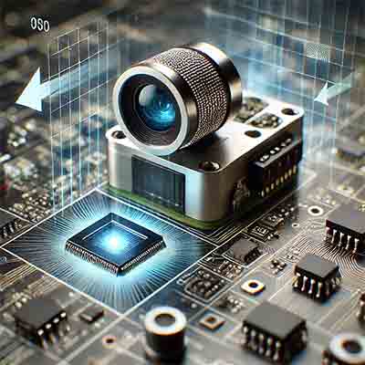
An optical flow sensor is a device that measures the motion of objects or surfaces within its field of view by detecting changes in the position of visual features over time. This sensor captures and analyzes the flow of light patterns to determine the direction and speed of movement.
Key Components:
- Imaging Sensor: Typically a camera or a photodetector array that captures
 sequential images or frames of the scene.
 - Processing Unit: Analyzes the captured images to calculate the optical flow, which is the apparent motion of objects, surfaces, and edges in a visual scene caused by the relative motion between an observer (the sensor) and the scene.
How It Works:
- Image Capture: The imaging sensor takes a series of images at different time intervals.
- Feature Detection: Key visual features, such as edges, corners, or textures, are identified in the images.
- Motion Estimation: The processing unit tracks the movement of these features across the sequence of images to estimate the direction and velocity of the motion.
Applications:
- Robotics: For navigation, obstacle avoidance, and motion control.
- Drones and UAVs: To stabilize flight and enable precise maneuvering.
- Computer Vision: In object tracking, motion detection, and video analysis.
- Gaming and Virtual Reality: For gesture recognition and immersive experiences.
Advantages:
- Real-time Processing: Allows for immediate detection and response to motion.
- Non-contact Measurement: Does not require physical contact with the moving object or surface.
- Versatility: Can be used in various environments and applications, from indoor robotics to outdoor navigation.
In summary, an optical flow sensor is a crucial tool in many advanced technological applications, providing accurate and real-time motion detection and analysis.
What Is An Optical Dissolved Oxygen Sensor
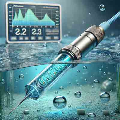
An optical dissolved oxygen sensor is a device that measures the concentration of dissolved oxygen in water using optical methods. These sensors are used in various applications, including environmental monitoring, aquaculture, wastewater treatment, and scientific research.
Key Components:
- Sensing Element: Contains a luminescent or fluorescent material that reacts to
 oxygen. Common materials include certain dyes or phosphorescent compounds.
 - Light Source: An LED or laser that emits light at a specific wavelength to excite the luminescent material.
- Photodetector: Detects the light emitted by the luminescent material after excitation.
- Optical Fiber: Often used to transmit light between the sensor and the water sample.
How It Works:
- Excitation: The light source emits light that excites the luminescent material in the sensing element.
- Luminescence: The luminescent material emits light in response to the excitation. The characteristics of this emitted light (intensity, phase shift, or lifetime) change depending on the amount of oxygen present.
- Detection: The photodetector measures the emitted light. The sensor's electronics then analyze these measurements to determine the concentration of dissolved oxygen.
Advantages:
- High Accuracy and Precision: Optical sensors are often more accurate and precise than traditional electrochemical sensors.
- Low Maintenance: These sensors typically require less maintenance since they don't consume oxygen and have fewer moving parts.
- Stable Readings: They provide stable readings over time, even in varying temperature and salinity conditions.
- Non-Invasive: The optical method is non-invasive, which means it doesn't alter the sample being measured.
Applications:
- Environmental Monitoring: Used to measure oxygen levels in rivers, lakes, and oceans for assessing water quality.
- Aquaculture: Helps in maintaining optimal oxygen levels in fish farms.
- Wastewater Treatment: Monitors oxygen levels to ensure proper aeration and treatment processes.
- Laboratory Research: Utilized in scientific studies involving oxygen consumption and production in biological samples.
In summary, an optical dissolved oxygen sensor is a sophisticated tool for accurately measuring dissolved oxygen levels in water through optical methods, offering advantages in accuracy, maintenance, and stability over traditional sensors.
