
While we have got some promising results for growth on GaN, we are still studying what happens when we try to grow on AlN. So that's why there is some delay on placing the orders. Once we have established that the 2D materials can be grown on onto these semiconductors, then i will go forward with the orders. I also see that u have graphene on SiO2/Si that also another substrate that i am keen on exploring with regards to 2D TMDC.
Gallium Nitride Template Applications
Gallium nitride templates are suitable for the fabrication of semiconductor devices. They can be fabricated with high-quality laser sintering techniques, and they are very versatile. They are available in different sizes and types, and can be used for many different applications. The main advantage of gallium nitride templates is their superior lattice matching properties, making them suitable for LED fabrication.
Get Your Quote FAST! Or, Buy Online and Start Researching Today!
What are GaN and AlN Templates Used For?
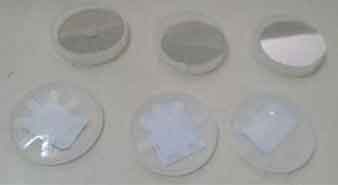
A researcher has informed us of his current template use:
LED Epitaxy Grown on GaN
Rsearcher asks:
UniversityWafer RFQ#253397 Response:
GaN-on-GaN 2” blue LED wafers. the whole substrate is Gallium Nitride. Blue wavelength 445~465nm
Contact us for pricing.
Overview of SiC and GaN Devices
Related GaN & Wide Bandgap Resources
Gallium Nitride (GaN) Templates
 GaN templates,
AlN templates are both available. Researchers use the templates to grow 2D transition metal dichalcogenides and measure their electrical properties. The templates are highly insulating with negligible electrical mobilities. This prevents spurious electrical signal to the 2D materials on surface.
GaN templates,
AlN templates are both available. Researchers use the templates to grow 2D transition metal dichalcogenides and measure their electrical properties. The templates are highly insulating with negligible electrical mobilities. This prevents spurious electrical signal to the 2D materials on surface.
For semi insulating GaN templates, the typical specifications are as follows. Size = 2", Single crystal/highly epitaxial grown on cAl2O3, single side polished, resistivity > or ~ 10^6 ohm cm. Quantity = 1-2 pieces. (based on price per piece). Please tell me if Gallium polar or Nitrogen polar can be obtained.
For semi insulating AlN templates, the typical specifications are as follows. Size = 2", Single crystal/highly epitaxial grown on
cAl2O3, single side polished. resistivity > 1 x 10^6 ohm cm. Quantity = 1-2 pieces. (based on price per piece). Please tell me if Aluminium polar or Nitrogen polar can be obtained.
For hBN, the typical specifications are as follows. Size = 10 mm x 10 mm pieces on
SiO2/Si. Resistivity > 1 x 10^6 ohm cm. Quantity = 5-10 pieces (based on price per piece).
Semi-Insulating GaN Template Inventory
Below are just some of our stock.
For semi insulating GaN templates, the typical specifications are as follows.
Size = 2", Single crystal/highly epitaxial grown on
cAl2O3, single side polished, resistivity > or ~ 10^6 ohm cm. Quantity = 1-2 pieces. Gallium polar,GaN layer 4~5um
Aluminum Nitride (AlN) Templates
For semi insulating AlN templates, the typical specifications are as follows.
Size = 2", Single crystal/highly epitaxial grown on
cAl2O3, single side polished. resistivity > 1 x 10^6 ohm cm. Quantity = 1-2 pieces. Aluminium polar,AlN layer 100nm
or semi insulating AlN templates, the typical specifications are as follows.
Size = 2", Single crystal/highly epitaxial grown on
cAl2O3, single side polished. resistivity > 1 x 10^6 ohm cm. Quantity = 5 pieces. Aluminium polar,AlN layer 1~2um
For semi insulating AlN templates, the typical specifications are as follows.
Size = 2", Single crystal/highly epitaxial grown on
cAl2O3, single side polished. resistivity > 1 x 10^6 ohm cm. Quantity = 5 pieces. Aluminium polar,AlN layer 4~5um
What Semiconductor Devices Use Gallium Nitride Templates?
Gallium nitride (GaN) is a semiconductor material that is used in semiconductor devices. The main characteristic of GaN is its high crystalline quality. Its good crystalline quality is beneficial for the light extraction process of light-emitting diodes. In order to avoid the negative influence of sapphire substrate on GaN growth, a silicon dioxide mask was deposited on the lenses. X-ray diffraction measurements showed that a single-crystal growth of GaN template occurred under the presence of SiO2 mask.
The conductive and insulating properties of GaN are mainly attributed to their low mobility. This feature is beneficial for semiconductor devices. The limiting factors of GaN are their high lattice mismatch and poor thermal conductivity. Hence, GaN and AlN templates can be used for the fabrication of various LED devices. The two materials are ideal for LEDs because they are both very effective in light and heat.
Gallium nitride templates are a type of semiconductor that is used to make LEDs and laser diodes. It has high atomic bonds and is good for semiconductor devices. Its low thermal conductivity and anti-radiation properties make it an excellent material for LEDs. They can be used to make blue and green LEDs, ultra-violet light detectors, and high-frequency power electronics.
Gallium nitride templates are suitable for the fabrication of semiconductor devices. They can be fabricated with high-quality laser sintering techniques, and they are very versatile. They are available in different sizes and types, and can be used for many different applications. The main advantage of gallium nitride templates is their superior lattice matching properties, making them suitable for LED fabrication.
Gallium nitride templates are a common material used in semiconductor devices. They are useful for LEDs and laser diodes as they improve the output of the LEDs when they are used in the green and yellow parts of the spectrum. But they also have a drawback. They have an extremely large lattice mismatch between their substrates and the light-emitting device, and they have a short life.
Indium gallium nitride templates are useful for semiconductor devices. They help address the long-standing problem of the "green gap" - where the yellow and green parts of the spectrum are not sufficiently compatible. Since the lattices of these materials are compatible with those of other metals, they can be used in LEDs. Then, they can be used as semiconductors in a variety of electronic applications.
The Gallium nitride templates are an excellent choice for LED structures. They are a good choice for this application because they can solve the long-standing problem of the "green gap" - in which the yellow and green parts of the spectrum are less compatible with the indium-based substrates. Indium gallium nitride templates have a much smaller lattice mismatch and thus have improved LED performance.
Gallium nitride templates are useful substrates for LED structures. They can also help address the long-standing problem of the "green gap". This problem affects LEDs' performance in the green and yellow parts of the spectrum. The indium gallium nitride template addresses this problem by reducing the mismatch between the two metals. The resulting crystalline GaN templates are an effective way to produce high-quality, high-efficiency LEDs.
The Gallium nitride template is a great option for LED structures. They can solve the long-standing problem of the "green gap" - when the LED emits in the green part of the spectrum, its output suffers. Due to this, gallium nitride templates are useful for addressing this problem. The advantages of this material are numerous. The indium nitride template are better suited for the semiconductor industry.
Indium nitride templates were developed in this way. They had a low indium content compared to GaN, which was the most common material. This difference was caused by the oxidation and nitride structure of the GaN. Both materials had the same hole concentration, but the nitride templates differed in the level of dopants. Moreover, p-SB has higher surface roughness than GaN.