Do you have the following?
150mm Sapphire Substrate 0.70mm Thickness Rounded Chamfer Single Side polish qty=25
A PhD fabricating wireless communications devices requested a quote for the following:
Do you have the following?
150mm Sapphire Substrate 0.70mm Thickness Rounded Chamfer Single Side polish qty=25
UniversityWafer, Inc. Quoted:
150mm Sapphire Substrate 0.625mm Thickness Rounded Chamfer Single Side polish Qty=25
High Purity(>99.996%)and Monocrystaline Al2O3
Surface:C-axis<0001>Tilt 0.2°± 0.1°towards M-axis
Primary flat:A-Plane(11-20) ± 0.3°
Flat cut:47.5 ± 2.5 mm
Dia.150.0 ± 0.2 mm
Thickness:625 ± 25 um
TTV/BOW/WARP= 20 um
Front Side:Epi-Ready Polished,Ra = 0.3 nm
Back Side:Fine Ground,Ra = 0.6~ 1.4um
Free of foreign materials,No Scratch,Crack,Pores,Twins
Wafer Edge:R-type
Laser Mark:None
Packaged in a class 100 clean Room,25 pcs Epi-ready Wafer in one Cassette under Nitrogen Atmosphere
Qty. 25pcs
Reference #304028 for specs and pricing.
Get Your Quote FAST! Or, Buy Online and Start Researching Today!
Our sapphire wafers have tight total thickness variation (TTV) and low roughness. Please send us your specs and quantity for an immediate quote.
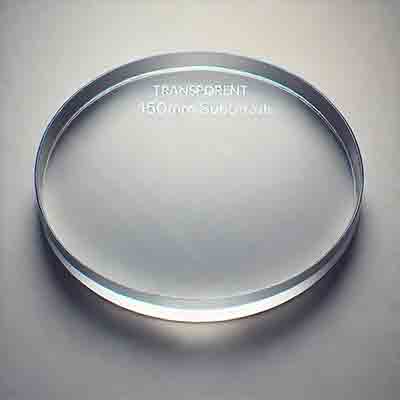
Below is just an example of the 150mm Sapphire that we sell.
6" R-Plane Sapphire Wafer,Single Side Polish
Type: CZ Grown Substrate
Diameter: 150 +/- 0.3mm
Surface Orientation: R-Plane(11-02): +/-1°
Primary Flat Orientation: 45° +/-2° CCW off C-axis projection on R-plane
Primary Flat Length: 47.5 +/-2.5 mm
Thickness: 0.60 +/- 0.025mm
TTV: </=20 μm
BOW: </=25 μm
WARP: </=40 μm
Surface finish (1 side): Epi-polished Ra</=0.3 nm
Surface finish (2 side): fine ground Ra </=1.0 um
Chamfer: Rounded
Laser marking: B/S
Package: Clean room,25pcs wafer in cassette vacuum sealed
150mm sapphire wafers are commonly used in a variety of high-tech applications due to their unique properties, including high thermal conductivity, chemical stability, and excellent optical clarity. Here are some key uses:
LED Manufacturing: Sapphire wafers serve as the substrate for growing gallium nitride (GaN) layers, which are essential for producing blue and white LEDs.
Semiconductor Devices: They are used as substrates in the fabrication of various semiconductor devices, including integrated circuits (ICs) and power electronics, due to their excellent insulating properties and high-temperature stability.
Optoelectronics: Sapphire wafers are used in optoelectronic devices such as laser diodes, photodetectors, and other components that require a transparent and durable substrate.
RFICs (Radio Frequency Integrated Circuits): Sapphire's high dielectric constant and low loss tangent make it suitable for RFIC applications, where it supports high-frequency operations with minimal signal loss.
Watch Crystals and Windows: Due to its hardness and scratch resistance, sapphire is often used for watch crystals and other durable, transparent windows in scientific and industrial equipment.
Optical Components: Sapphire wafers are used in the production of optical components such as lenses, prisms, and windows, particularly in harsh environments where durability is crucial.
MEMS Devices: Micro-Electro-Mechanical Systems (MEMS) devices often use sapphire substrates for their mechanical strength and stability.
These applications leverage sapphire's robustness, thermal properties, and optical clarity, making it an indispensable material in various advanced technological fields.