
What Is Graphene?
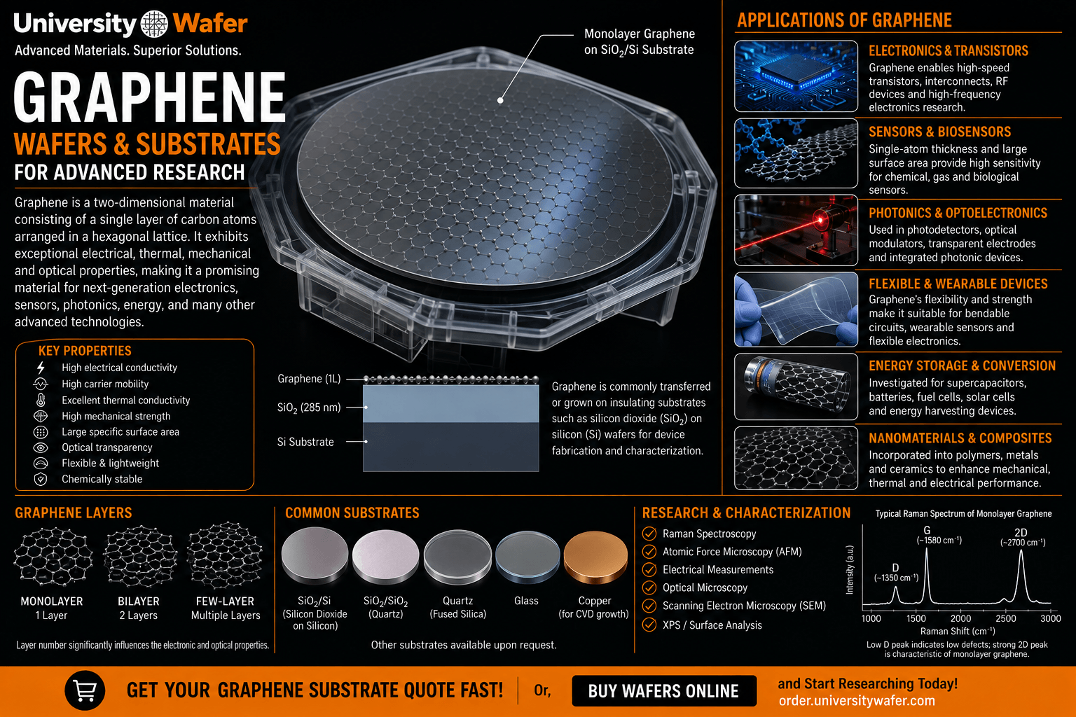
Graphene is a two-dimensional material consisting of a single layer of carbon atoms arranged in a hexagonal lattice. Despite being only one atom thick, graphene combines exceptional electrical, thermal, mechanical, and optical properties that make it an important material for advanced research and next-generation device development.
UniversityWafer supplies graphene materials and graphene-coated substrates for universities, research laboratories, semiconductor developers, and industrial R&D. Graphene can be investigated for electronics, sensors, photonics, nanotechnology, flexible devices, energy storage, and other emerging technologies.
Why Is Graphene Important?
Graphene's unusual combination of properties has made it one of the most extensively researched two-dimensional materials. Its atomic-scale thickness allows researchers to investigate electronic and physical behavior that differs significantly from conventional bulk materials.
Important graphene properties include:
- High carrier mobility: Attractive for high-speed electronic and transport research.
- Excellent thermal conductivity: Useful for studying heat spreading and thermal-management technologies.
- High mechanical strength: Graphene combines exceptional strength with extremely low thickness.
- Large surface-to-volume ratio: Valuable for chemical, biological, and environmental sensor research.
- Optical transparency: Enables research into transparent electrodes, photonics, and optoelectronic devices.
- Mechanical flexibility: Useful for flexible and wearable electronic research.
Graphene Crystal Structure
Graphene consists of sp2-bonded carbon atoms arranged in a two-dimensional honeycomb lattice. This atomic structure is responsible for many of graphene's distinctive electronic and mechanical characteristics.
A single graphene sheet can also be considered the fundamental structural building block of several other carbon materials. Stacking graphene layers produces graphite, while graphene can also be conceptually related to carbon nanotubes and other nanoscale carbon structures.
CVD Graphene
Chemical Vapor Deposition (CVD) graphene is widely used when relatively large-area graphene films are required. During CVD growth, carbon-containing precursor gases are introduced into a controlled environment where graphene forms on a suitable catalytic surface, commonly a metal such as copper.
The graphene film can subsequently be transferred onto another substrate for device fabrication and characterization. Depending on the research requirements, graphene may be transferred onto silicon wafers, silicon dioxide, glass, quartz, or other experimental substrates.
Graphene on Silicon & SiO2
Graphene on silicon substrates provides a convenient platform for electronic, optical, and materials-science research. Silicon wafers with a silicon dioxide layer are particularly common because the oxide electrically isolates graphene from the underlying silicon and can assist with optical characterization.
Researchers requiring oxide-coated substrates can explore thermal oxide silicon wafers for graphene transfer, device fabrication, and thin-film experiments.
Monolayer & Few-Layer Graphene
The number of graphene layers can significantly affect material behavior. Monolayer graphene consists of one atomic carbon layer, while bilayer and few-layer graphene contain additional stacked sheets.
Researchers should consider layer count when selecting graphene because electronic, optical, and transport characteristics can change as additional layers are introduced.
Graphene for Electronic Devices
Graphene's carrier transport properties make it attractive for research into high-speed and nanoscale electronics. Researchers investigate graphene for field-effect transistors, interconnects, conductive films, RF devices, and other experimental electronic structures.
Graphene does not behave like conventional silicon and has no intrinsic bandgap in its ideal monolayer form, which presents challenges for conventional digital switching. However, its electronic properties remain valuable for specialized high-frequency, sensing, and transport applications.
Graphene Sensors
The extremely high surface-to-volume ratio of graphene makes its electrical properties sensitive to interactions occurring at the material surface. This characteristic is valuable for chemical, gas, biological, and environmental sensor research.
Potential graphene sensor applications include:
- Gas detection
- Chemical sensing
- Biosensors
- Environmental monitoring
- Strain and pressure sensing
- Optical sensing
Graphene for Photonics & Optoelectronics
Graphene combines electrical conductivity with optical properties that make it interesting for photonics and optoelectronic research. Experimental applications include photodetectors, optical modulators, transparent conductive layers, and integrated photonic structures.
Its broadband optical interaction also allows graphene to be investigated across wavelength ranges relevant to visible, infrared, and other photonic technologies.
Flexible & Transparent Electronics
Because graphene is extremely thin and mechanically flexible, it is studied for flexible and transparent electronic devices. Conductive graphene films may be incorporated into experimental displays, wearable sensors, flexible circuits, transparent electrodes, and other emerging devices.
Researchers working with flexible device architectures can also explore flexible electronics substrates.
Graphene for Energy Research
Graphene and graphene-based structures are investigated for energy storage and conversion technologies. Their high surface area and electrical conductivity make them interesting for experimental electrodes and composite materials.
Research areas include batteries, supercapacitors, photovoltaic structures, fuel-cell components, and other next-generation energy technologies.
Graphene Characterization
Accurate characterization is important for determining graphene layer count, surface condition, defects, morphology, and material quality. Common research techniques can include Raman spectroscopy, optical microscopy, electron microscopy, electrical measurements, and Atomic Force Microscopy (AFM).
Selecting a Graphene Substrate
The appropriate graphene substrate depends on the intended experiment and fabrication process. Researchers may need to consider:
- Monolayer or few-layer graphene
- Graphene growth or transfer method
- Substrate material
- Silicon dioxide thickness
- Graphene coverage and dimensions
- Surface cleanliness
- Electrical properties
- Required characterization
- Device fabrication compatibility
Clearly defining the graphene layer and underlying substrate specifications helps ensure compatibility with lithography, deposition, electrical measurements, microscopy, and other downstream research processes.
Get Your Graphene Wafer & Substrate Quote FAST! Or, Buy Wafers Online and Start Researching Today!
Graphene Applications & Emerging Technologies
Graphene materials and substrates are being investigated across electronics, biotechnology, photonics, energy storage, sensors, flexible devices, and nanotechnology. Its combination of atomic-scale thickness, electrical conductivity, mechanical strength, and large surface area allows researchers to explore device architectures that are difficult to achieve using conventional bulk materials.
Graphene Field-Effect Transistors (GFETs)
Graphene can be incorporated into graphene field-effect transistors (GFETs), where a graphene channel responds to changes in an applied electric field. The high carrier mobility of graphene makes these structures especially interesting for high-frequency electronics, sensors, and fundamental charge-transport research.
Researchers studying transistor technologies can also explore field-effect transistor (FET) research and semiconductor substrate requirements.
Graphene Biosensors
The large exposed surface area of graphene makes it particularly interesting for biosensor development. Molecules interacting with a graphene surface can influence its electrical characteristics, allowing researchers to investigate highly sensitive detection techniques.
Potential research applications include:
- Biomolecular detection
- DNA and protein sensing
- Chemical detection
- Gas sensors
- Environmental monitoring
- Lab-on-a-chip devices
- Electrochemical sensors
Graphene Photodetectors
Graphene is investigated for photodetectors and optoelectronic devices because it can interact with light across a broad range of wavelengths. Researchers can integrate graphene with semiconductor or photonic structures to study high-speed optical detection and light-matter interactions.
Transparent Conductive Electrodes
Graphene's combination of optical transparency and electrical conductivity makes it a candidate for transparent electrode research. Thin graphene films can potentially provide electrical conduction while allowing a substantial portion of incident light to pass through the structure.
Potential applications include displays, touch interfaces, photovoltaic devices, optical sensors, and flexible electronics. Researchers requiring established transparent conductive coatings may also consider ITO-coated wafers and substrates.
Flexible & Wearable Devices
Unlike brittle bulk materials, atomically thin graphene can tolerate substantial bending when properly supported. This makes it attractive for flexible electronics and wearable sensor research.
Graphene may be transferred onto polymers and other flexible materials to investigate bendable circuits, strain sensors, wearable electronics, transparent conductors, and flexible energy devices.
Explore additional substrates for flexible electronics when developing experimental device structures.
Graphene for RF & High-Frequency Electronics
The carrier transport properties of graphene have generated interest in radio-frequency (RF) and high-frequency electronics. Graphene-based transistors and related structures are researched for applications where rapid carrier transport is more important than conventional digital switching behavior.
Graphene in Batteries & Supercapacitors
Graphene's electrical conductivity and large specific surface area make it interesting for energy-storage research. Graphene and graphene-containing composites can be investigated as electrode materials and conductive additives in batteries and supercapacitors.
Research focuses on areas such as charge transport, electrode architecture, surface chemistry, energy density, power delivery, and cycle performance.
Graphene for Solar Cell Research
Graphene can also be investigated as a conductive or interfacial material in photovoltaic devices. Potential roles include transparent electrodes, charge-transport layers, and components of experimental heterostructures.
Researchers developing photovoltaic structures can explore additional wafers and substrates for solar-cell research.
Graphene Nanocomposites
Graphene can be incorporated into polymers, ceramics, metals, and other materials to create graphene-based nanocomposites. Researchers investigate these composites to modify electrical conductivity, thermal behavior, mechanical properties, and other material characteristics.
Graphene on SiO2/Si
Graphene on silicon dioxide/silicon (SiO2/Si) is a widely used research configuration. The oxide layer electrically separates graphene from the silicon substrate while providing a convenient surface for microscopy, lithography, electrical contacts, and device fabrication.
Researchers can select thermal oxide silicon wafers with oxide thicknesses appropriate for their graphene transfer and characterization requirements.
Graphene on Quartz & Glass
Transparent substrates can be useful when graphene experiments require optical access through the supporting material. Graphene transferred onto quartz substrates or glass can support research involving transparent electrodes, spectroscopy, optical sensors, and photonic devices.
Graphene Heterostructures
Graphene can be combined with other two-dimensional and semiconductor materials to create van der Waals heterostructures. Stacking atomically thin materials allows researchers to engineer interfaces and investigate new electronic, optical, and quantum phenomena.
These structures are studied for transistors, photodetectors, tunneling devices, sensors, quantum research, and other emerging nanoscale technologies.
Measuring Graphene Quality
Material characterization is important because defects, contamination, wrinkles, grain boundaries, and layer number can significantly affect graphene performance. Researchers may use several complementary techniques to evaluate graphene samples.
- Raman spectroscopy: Commonly used to investigate layer number, defects, strain, and doping.
- AFM: Measures surface morphology, roughness, and nanoscale height variations.
- Optical microscopy: Useful for locating transferred graphene and inspecting larger surface features.
- Electron microscopy: Provides high-resolution structural information.
- Electrical measurements: Used to characterize resistance, carrier transport, and device behavior.
Learn more about Atomic Force Microscopy (AFM) for nanoscale surface characterization.
Choosing Graphene for Your Research
When selecting graphene materials or graphene-coated substrates, researchers should consider both the graphene layer and the supporting substrate. Important specifications may include:
- Monolayer, bilayer, or few-layer graphene
- CVD-grown or other graphene type
- Graphene coverage area
- Substrate material
- Substrate dimensions
- SiO2 thickness when applicable
- Surface cleanliness
- Defect density and graphene quality
- Transfer requirements
- Electrical or optical characterization needs
Matching these specifications to the intended fabrication and characterization process can improve consistency when developing graphene electronics, sensors, photonic structures, and other nanoscale devices.
Related Graphene & Advanced Materials Research
- Graphene Wafers & Substrates
- Silicon Wafers
- Thermal Oxide Silicon Wafers
- Single Crystal Quartz Wafers
- Glass Wafers & Substrates
- ITO-Coated Wafers & Transparent Conductive Substrates
- Flexible Electronics Substrates
- Field-Effect Transistor (FET) Research
- Atomic Force Microscopy (AFM)
- Wafers for Solar Cell Research