
Buy "Golden Spec" 2D Substrates
Stop guessing with standard wafers. For 2D research, you need specific oxide thicknesses for visibility and high doping for conductivity. We have them in stock.
Best Sellers: 285nm Oxide + Back-Gate
These wafers allow you to see monolayers (purple/violet contrast) and use the substrate as a global back-gate (< 0.005 Ω·cm).
| Item ID | Size | Spec Highlights | Action |
|---|---|---|---|
| #1583 | 100mm (4") | P++ (Boron), 300nm Oxide, <0.005 Ω·cm | Buy Now |
| #3510 | 50.8mm (2") | P++ (Boron), 300nm Oxide, <0.005 Ω·cm | Buy Now |
| #1432 | 100mm (4") | Standard P-type, 300nm Oxide (Visibility Only) | Buy Now |
Note: 285nm is often listed as 300nm ± 5% in industry terms. Both provide excellent contrast for Graphene/MoS2.
Researcher Case Studies & RFQs
Microwells to Create Free-Standing 2D Materials
"We need silicon wafer pieces with spherical wells which have ~ 1 um diameter. Our aim is using such wells to create free-standing 2D materials for measuring their mechanical properties."
Assistant Professor | Reference #260344Sapphire Wafers for 2D Material Growth
"We are currently in search of sapphire substrates, specifically double-sided polished and fully transparent, for use as substrates in the growth of two-dimensional materials... we noticed available sizes are mainly 50mm and 100mm."
[Image of sapphire crystal structure] Doctoral Student | Reference #278810HOPG Substrates for Fabricating 2D Materials
"I'm looking to buy HOPG as a substrate for 2D materials. Could I have a quote for HOPG of size 10*10*0.5mm?"
PhD Candidate | Reference #255966Thermal Oxide for Growing 2D Materials
"We would like to make an order of '285nm SiO2 on Si' substrates for the growth of 2D materials. In fact, my colleague already contacted you and we learnt that 2 inch P(100) 1-10 ohm-cm SSP 500um with 285nm of oxide."
Assistant Professor | Reference #188309Photoemission Measurements (Defect Density)
"285nm oxide thickness desired... We do low temperature optical measurements and I've noticed that other SiO2/Si substrates can give fluorescence peaks that are due to defects. Can you quantify defect density in your wafers?"
Postdoc | Reference #209209WS2 and WSe2 2D Materials
"Please send me a quotation including... Bilayer Graphene on SiO2/Si (10 mm x 10 mm)... If you can provide other 2D materials, e.g. WS2 and WSe2, I am also interested."
PostDoc | Reference #215004Get a Custom Quote
Need custom alignment marks, 90nm oxide, or specific dicing?
Or, Buy Online and Start Your Research today!
Choosing Substrates for 2D Materials Research
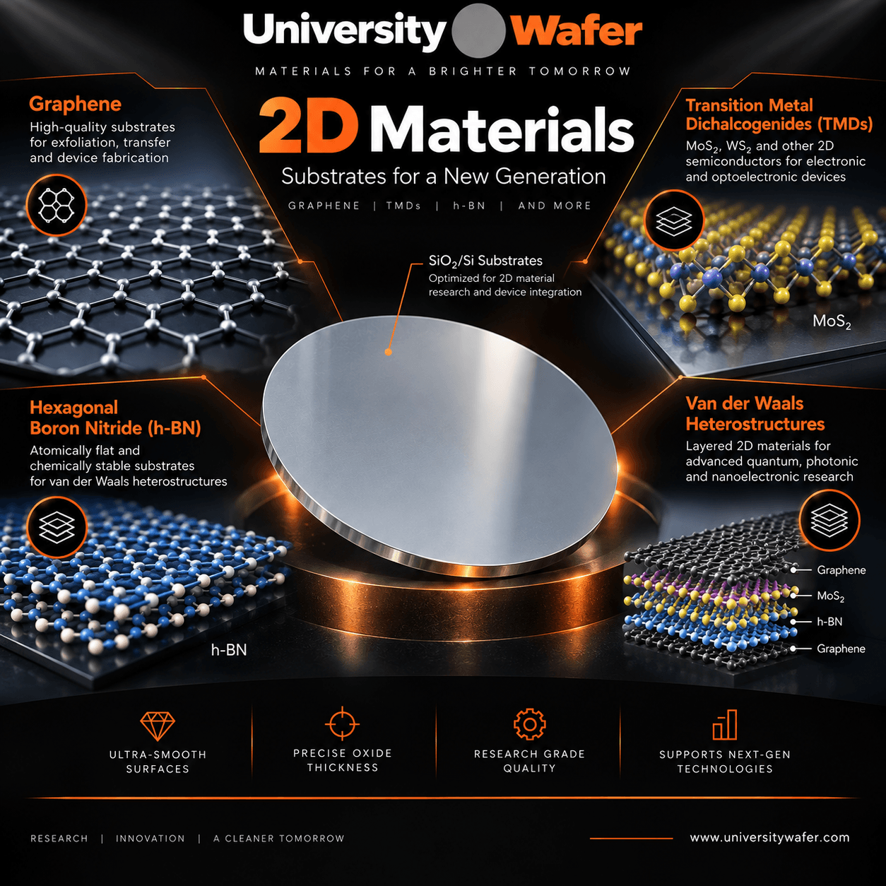
The substrate can strongly influence the visibility, transfer quality, electrical behavior, contamination level, and processing of atomically thin materials. UniversityWafer supplies silicon, SiO₂/Si, fused silica, quartz, sapphire, and other substrates used for graphene, transition-metal dichalcogenides (TMDs), h-BN, and other 2D materials.
The best substrate specification depends on whether your research involves mechanical exfoliation, material transfer, optical characterization, device fabrication, or high-temperature synthesis.
Why 285 nm SiO₂/Si Is Popular for 2D Materials
Monolayer and few-layer materials can be difficult to identify because they absorb only a small fraction of visible light. A thermally oxidized silicon wafer can enhance their optical contrast through thin-film interference, making flakes easier to locate with an optical microscope.
Approximately 285 nm SiO₂ is widely used for graphene and other exfoliated 2D materials. Approximately 90 nm SiO₂ is another common choice. The optimum oxide thickness and illumination conditions depend on the material, wavelength, microscope configuration, and number of layers.
Conductive Silicon for Back-Gated Devices
For graphene, MoS₂, WS₂, and other 2D-material field-effect devices, a heavily doped silicon substrate beneath the SiO₂ dielectric can serve as a global back-gate electrode. This configuration is widely used for research devices because it simplifies fabrication and enables researchers to tune carrier density electrically.
- Simplified Device Fabrication: Heavily doped silicon can function as a common back gate, reducing the need for a separately patterned local gate in basic device structures.
- High-Quality Gate Dielectric: Thermally grown SiO₂ is valued for its dense structure, reproducible thickness, and well-characterized electrical properties.
- Research Flexibility: Oxide thickness and silicon resistivity can be selected to match optical, electrical, and device-processing requirements.
Which Substrate Should You Use?
Mechanical Exfoliation and Flake Transfer
For mechanical exfoliation of graphene, h-BN, MoS₂, WS₂, and related layered materials, researchers commonly use smooth prime-grade silicon wafers with a controlled thermal oxide layer.
Low surface roughness and a clean oxide surface help improve contact between the transferred flake and substrate. SiO₂ thickness can also be selected to improve optical contrast when locating thin flakes.
CVD Growth and High-Temperature Processing
Substrate selection for CVD growth depends strongly on the 2D material and synthesis chemistry. Thermally oxidized silicon, sapphire, quartz, and fused silica substrates are among the materials used in 2D-material research.
For elevated-temperature processes, researchers should consider thermal stability, surface chemistry, contamination, thermal expansion, substrate-film interactions, and compatibility with the growth atmosphere rather than selecting a substrate based on temperature alone.
Electrical Transport and FET Research
For back-gated 2D-material devices, a common platform consists of heavily doped Si with thermally grown SiO₂. The silicon acts as the back gate while the oxide provides electrical isolation between the gate and the 2D-material channel.
What Is 2D Material Exfoliation?
Exfoliation separates layered bulk crystals into thinner flakes, including few-layer and potentially monolayer materials. Layered crystals are particularly suitable for exfoliation because their atomic planes are held together by relatively weak van der Waals interactions.
- Mechanical Exfoliation: Often called the Scotch-tape method, mechanical exfoliation repeatedly cleaves a layered crystal before transferring thin flakes to a substrate. It is widely used when high crystal quality is more important than large-area coverage.
- Liquid-Phase Exfoliation: Layered materials are dispersed in a liquid and exfoliated using methods such as sonication or shear mixing. This approach can produce larger quantities of nanosheets, although the resulting material generally has a broader distribution of lateral size and layer thickness.
Recommended Silicon Wafer Parameters
There is no single silicon wafer specification that is optimal for every 2D material. Researchers should consider the following parameters when selecting a substrate:
- Oxide Thickness: Approximately 285 nm and 90 nm thermal SiO₂ are commonly selected when optical contrast is important.
- Silicon Resistivity: Heavily doped, low-resistivity silicon is useful when the substrate must function as a global back gate.
- Surface Quality: Prime-grade wafers provide smooth, clean surfaces suitable for exfoliation, transfer, lithography, and device fabrication.
- Wafer Orientation: Si(100) is widely available and commonly used for SiO₂/Si research substrates. Orientation becomes more important when crystal orientation or epitaxial relationships are relevant to the experiment.
- Thermal Oxide Quality: High-quality thermal SiO₂ provides controlled thickness and a stable dielectric surface for many electrical and optical experiments.
- Wafer Size and Thickness: Diameter and thickness should be selected for compatibility with transfer tools, lithography equipment, deposition systems, and other laboratory processes.
2D Materials Commonly Studied on Our Substrates
- Graphene: Frequently transferred or exfoliated onto SiO₂/Si for electronic transport, sensor, optical, and device research.
- MoS₂ and WS₂: Semiconducting transition-metal dichalcogenides widely investigated for transistors, photodetectors, optoelectronics, and heterostructures.
- h-BN: A wide-bandgap layered material commonly used as an insulating layer, encapsulation material, or atomically smooth dielectric in van der Waals heterostructures.
- Graphite and HOPG: Layered carbon materials used as starting materials for exfoliation and as substrates or reference surfaces in scanning probe research.
Building Van der Waals Heterostructures
Researchers can stack graphene, h-BN, TMDs, and other atomically thin materials to create van der Waals heterostructures. These structures allow materials with different electronic, optical, and dielectric properties to be combined without requiring conventional lattice-matched epitaxy.
High-quality substrates provide the foundation for these experiments by supporting controlled transfer, optical identification, lithography, electrical measurements, and subsequent device fabrication.
Related 2D Materials & Substrate Resources
- Graphene Substrates – Explore substrates used for graphene exfoliation, transfer, characterization, and device research.
- Van der Waals Materials – Learn how weak interlayer interactions enable exfoliation and stacked 2D heterostructures.
- Prime Grade Silicon Wafers – High-quality silicon surfaces for 2D material transfer, lithography, and device fabrication.
- Silicon Wafers – Browse silicon substrates with different orientations, resistivities, diameters, and surface specifications.
- Dielectric Materials – Learn about dielectric layers used in gates, insulation, and advanced semiconductor devices.
- Chemical Vapor Deposition (CVD) – Explore CVD processes relevant to thin films and 2D material synthesis.
- Fused Silica Wafers – Optical and thermally stable substrates for materials science and thin-film research.
- Sapphire Substrates – Explore crystalline sapphire substrates for thin-film growth and advanced materials research.