
Semiconductor Wafers & Substrates for Research
UniversityWafer supplies a broad selection of semiconductor wafers and substrates for university research, semiconductor development, prototyping, MEMS, photonics, optoelectronics, power electronics, sensors, and other advanced materials applications.
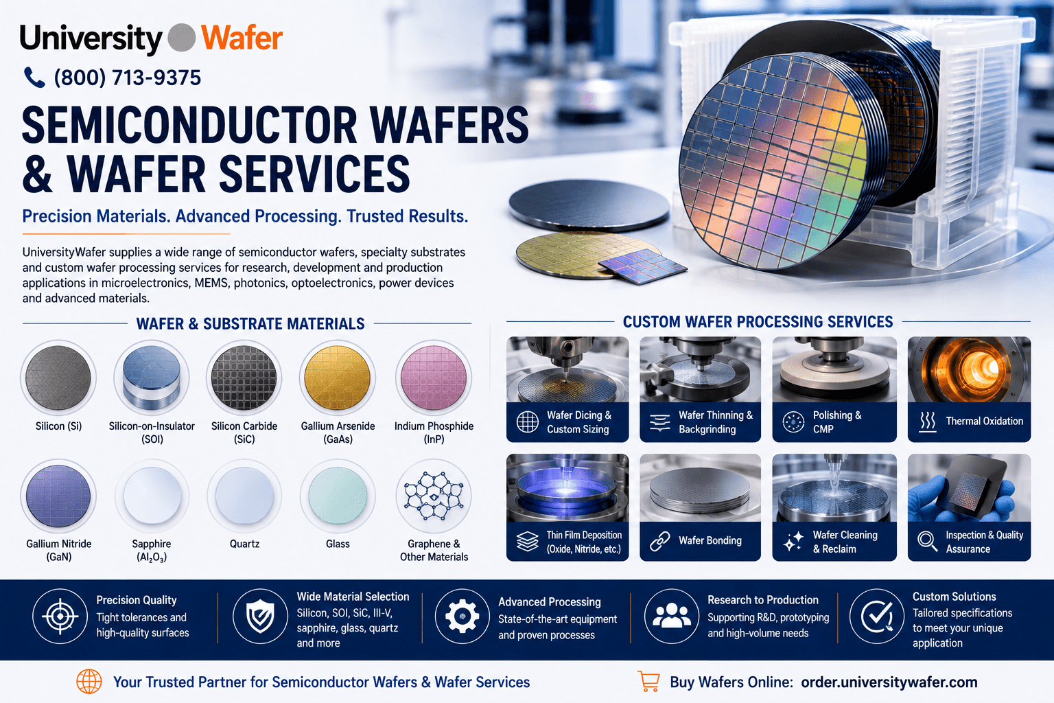
Available substrate materials include silicon (Si), silicon-on-insulator (SOI), silicon carbide (SiC), gallium arsenide (GaAs), indium phosphide (InP), gallium nitride (GaN), sapphire (Al₂O₃), germanium, glass, quartz, and other specialty materials. Because each material has different electrical, optical, thermal, mechanical, and crystallographic properties, the correct substrate should be selected according to the intended device and fabrication process.
Silicon Wafers for Semiconductor Fabrication
Silicon wafers remain the most widely used semiconductor substrates for integrated circuits, MEMS, sensors, photovoltaics, microfluidics, thin-film research, and many other microfabrication applications.
Silicon substrates can be specified by diameter, thickness, crystal orientation, conductivity type, dopant, resistivity, surface finish, and other parameters. Common crystal orientations include (100), (111), and (110), with the appropriate orientation depending on the fabrication process and device requirements.
Researchers can select P-type, N-type, undoped or high-resistivity material as required. Single-side polished (SSP) and double-side polished (DSP) wafers are also available for applications requiring different surface conditions.
Silicon-on-Insulator (SOI) Wafers
Silicon-on-insulator (SOI) wafers consist of a silicon device layer separated from a silicon handle wafer by an insulating buried oxide (BOX) layer. This engineered structure provides electrical isolation and can reduce parasitic capacitance in appropriate electronic devices.
SOI substrates are widely used in MEMS, CMOS research, RF electronics, integrated photonics, sensors, and microfluidic structures. Important SOI specifications include device-layer thickness, buried-oxide thickness, handle-wafer properties, crystal orientation, resistivity, and surface finish.
Silicon Carbide Wafers for Power Electronics
Silicon carbide (SiC) wafers are wide-bandgap semiconductor substrates used extensively in research involving high-power, high-voltage, high-temperature, and RF electronic devices.
4H-SiC is the dominant SiC polytype for many modern power-electronic devices because of its wide bandgap, high critical electric field, and high thermal conductivity. SiC substrates can also support epitaxial layers used to fabricate MOSFETs, Schottky diodes, and other power semiconductor structures.
III-V Semiconductor Wafers
UniversityWafer supplies III-V semiconductor substrates for applications where silicon does not provide the required optical or electronic properties. Common materials include gallium arsenide (GaAs), indium phosphide (InP), indium arsenide (InAs), gallium antimonide (GaSb), and related compound semiconductor structures.
Many III-V semiconductors have direct bandgaps and favorable carrier transport properties, making selected materials useful for LEDs, laser diodes, photodetectors, solar cells, RF electronics, high-speed transistors, infrared devices, and integrated photonics.
Gallium Arsenide (GaAs) Substrates
Gallium arsenide (GaAs) wafers are direct-bandgap III-V semiconductor substrates used in RF, microwave, optoelectronic, laser, LED, and photovoltaic research.
GaAs has substantially higher electron mobility than silicon at room temperature, which can be advantageous for selected high-frequency electronic devices. Its direct bandgap also enables efficient light-emitting and light-absorbing semiconductor structures.
Indium Phosphide (InP) Wafers
Indium phosphide (InP) substrates are important for high-speed electronics and photonic devices, particularly technologies operating at wavelengths used in optical communications.
InP can serve as a substrate for epitaxial structures containing materials such as InGaAs and InGaAsP. These heterostructures are used in lasers, photodiodes, modulators, high-speed transistors, and other optoelectronic devices.
Sapphire Wafers & Substrates
Sapphire wafers are single-crystal aluminum oxide (Al₂O₃) substrates valued for their electrical insulation, hardness, chemical stability, and optical transparency over a broad wavelength range.
Sapphire is widely used as a substrate for GaN epitaxy in LED and optoelectronic research and is also used for optical windows, RF applications, sensors, thin-film deposition, and other demanding research environments.
Glass, Quartz & Optical Substrates
UniversityWafer supplies glass wafers and quartz substrates for microfluidics, MEMS, sensors, displays, thin-film deposition, photonics, and optical research.
Available materials can include fused silica and several engineered glasses. Material selection should consider optical transmission, coefficient of thermal expansion, chemical durability, surface quality, softening temperature, and compatibility with the intended fabrication process.
Custom Wafer Processing Services
Substrate preparation often requires more than selecting the starting wafer. UniversityWafer provides custom wafer processing services for researchers who require modified dimensions, surfaces, dielectric layers, or other substrate specifications.
Processing capabilities can include:
- Wafer dicing and custom-sized pieces
- Wafer thinning and backgrinding
- Single-side and double-side polishing
- Thermal oxidation
- Silicon nitride deposition
- Thin-film and specialty coatings
- Wafer bonding
- Wafer reclaim and surface preparation
Wafer Dicing & Custom-Sized Substrates
Wafer dicing services allow full wafers to be divided into smaller dies, chips, rectangles, or other specified dimensions. Diced substrates are useful when experiments do not require a full wafer or when samples must fit specialized holders, deposition equipment, microscopes, or testing systems.
Dicing requirements should account for substrate material, thickness, desired dimensions, edge quality, surface coatings, and any fragile structures already present on the wafer.
Wafer Thinning & Backgrinding
Silicon wafer backgrinding and thinning can reduce substrate thickness for MEMS, packaging, flexible-device research, sensors, and other applications where the standard wafer thickness is not suitable.
Mechanical grinding can introduce subsurface damage and stress, so additional lapping, polishing, or chemical processing may be required when a high-quality finished surface is needed.
Wafer Polishing & Surface Preparation
Semiconductor fabrication frequently requires smooth, flat surfaces for lithography, thin-film deposition, bonding, epitaxy, and device processing. Wafer polishing can improve surface roughness and remove damage introduced during slicing, grinding, or other mechanical operations.
For applications requiring highly planar surfaces, chemical mechanical polishing (CMP) combines chemical reactions with controlled mechanical abrasion to remove material and improve surface planarity.
Thermal Oxide & Dielectric Wafers
UniversityWafer supplies thermal oxide silicon wafers with silicon dioxide (SiO₂) layers for semiconductor devices, MOS structures, MEMS, sensors, microfluidics, thin-film research, and dielectric studies.
Thermally grown SiO₂ is produced by oxidizing the silicon surface at elevated temperature in dry oxygen or water-vapor-containing ambients. Oxide thickness and growth method should be selected according to the electrical, optical, and processing requirements of the application.
Wafer Bonding Services
Wafer bonding can join two substrates to form engineered structures for MEMS, microfluidics, sensors, SOI-related research, packaging, and other microfabricated devices.
Bonding techniques can include direct or fusion bonding, anodic bonding, and adhesive approaches depending on the materials and application. Surface roughness, cleanliness, flatness, thermal-expansion compatibility, and processing temperature are important considerations when selecting a bonding process.
How to Specify Semiconductor Wafers
Selecting a semiconductor wafer or specialty substrate requires matching the material and specifications to the intended fabrication process. Important parameters can include:
- Material: Si, SOI, SiC, GaAs, InP, sapphire, glass, quartz, or another substrate
- Diameter and dimensions: full wafer, diced chip, or custom geometry
- Thickness: standard or custom-thinned material
- Crystal orientation: such as (100), (110), (111), or material-specific planes
- Doping: conductivity type, dopant species, and concentration when applicable
- Resistivity: selected according to electrical requirements
- Surface finish: SSP, DSP, epitaxy-ready, or other specified preparation
- Thin films: oxide, nitride, metals, or other deposited layers
- Flatness and surface quality: TTV, bow, warp, and roughness when critical
Providing complete specifications helps ensure that the selected semiconductor substrate is compatible with the intended lithography, deposition, etching, epitaxy, bonding, MEMS, photonic, or electronic device process.
Get Your Semiconductor Wafer & Wafer Services Quote FAST! Or, Buy Wafers Online and Start Researching Today!
Choosing the Right Wafer for Your Research
Selecting the correct semiconductor wafer requires more than choosing a substrate material. Crystal orientation, diameter, thickness, doping, resistivity, surface finish, flatness, deposited films, and thermal-processing requirements can all influence fabrication results and device performance.
UniversityWafer supplies semiconductor wafers and substrates for research involving microelectronics, MEMS, photonics, sensors, optoelectronics, power electronics, thin films, and advanced materials. Substrate specifications should be selected according to the physical requirements of the experiment rather than assuming that one wafer grade is appropriate for every application.
Semiconductor Wafer Crystal Orientation
Crystal orientation describes the crystallographic plane parallel to the wafer surface. For single-crystal silicon, common wafer orientations include (100), (110), and (111). Orientation can influence surface atomic structure, oxidation behavior, anisotropic etching, mechanical properties, epitaxial relationships, and device fabrication.
(100) silicon is widely used for integrated-circuit and MOS research, while (111) and (110) substrates are useful for applications requiring different surface symmetry, etching behavior, or crystallographic properties.
Researchers working with orientation-dependent processes can explore silicon wafers in multiple orientations, diameters, thicknesses, resistivities, and surface finishes.
P-Type and N-Type Silicon Wafers
Silicon conductivity is intentionally modified by introducing controlled concentrations of electrically active dopants. Common P-type silicon uses acceptor dopants such as boron, while N-type silicon commonly uses donor dopants such as phosphorus, arsenic, or antimony.
Doping changes the equilibrium concentration of free charge carriers and therefore affects electrical resistivity and semiconductor behavior. Researchers should specify conductivity type, dopant species, and resistivity according to the electrical requirements of the intended device.
Learn more about P-type silicon wafers and semiconductor doping for electronic-device and materials research.
Wafer Resistivity & Carrier Concentration
Wafer resistivity is an important electrical specification for semiconductor substrates. In doped semiconductors, resistivity depends on carrier concentration and carrier mobility, both of which can vary with dopant concentration and temperature.
Low-resistivity wafers are useful when the substrate must provide significant electrical conduction, while high-resistivity silicon wafers can be advantageous for RF, microwave, detector, sensor, and selected photonic applications where substrate conduction or parasitic electrical loss should be minimized.
UniversityWafer can supply high-resistivity silicon wafers and heavily doped substrates for research requiring different electrical properties.
Single-Side vs. Double-Side Polished Wafers
Surface finish should be selected according to the fabrication process. Single-side polished (SSP) wafers provide a polished device surface while the backside may retain a rougher finish. Double-side polished (DSP) wafers provide polished surfaces on both sides.
DSP substrates can be advantageous for through-wafer optical experiments, double-sided lithography, wafer bonding, MEMS, microfluidics, and applications requiring tight thickness uniformity or controlled surfaces on both sides.
Additional chemical mechanical polishing (CMP) can be used when processes require improved planarity or a highly controlled surface finish.
Wafer Flatness, Bow, Warp & TTV
Geometric specifications become increasingly important for lithography, bonding, thin-film deposition, precision metrology, and other processes requiring consistent wafer positioning.
Total thickness variation (TTV) describes the difference between the maximum and minimum wafer thickness under a defined measurement condition. Bow and warp characterize different aspects of wafer shape and departure from an ideal reference plane. These parameters are related but should not be treated as interchangeable.
Applications involving precision bonding, optical structures, MEMS, or advanced lithography may require tighter geometric tolerances than general materials research.
Epitaxial Wafers for Semiconductor Devices
Epitaxy is the growth of a crystalline layer whose crystallographic relationship is controlled by the underlying crystalline substrate. Epitaxial layers can provide electrical, compositional, and structural properties different from those of the starting wafer.
Silicon epitaxial wafers are used in semiconductor-device research where controlled layer thickness, doping, and crystal quality are required. Compound semiconductor epitaxy is similarly important for LEDs, lasers, photodetectors, RF electronics, and other optoelectronic devices.
Epitaxial specifications can include layer thickness, dopant concentration, resistivity, composition, surface morphology, and substrate orientation.
Thin-Film Deposition on Semiconductor Wafers
Semiconductor wafers frequently serve as substrates for thin-film deposition . Films can provide dielectric, conductive, semiconducting, optical, protective, or functional properties depending on the material and deposition process.
Common deposition methods include chemical vapor deposition (CVD), plasma-enhanced chemical vapor deposition (PECVD), physical vapor deposition (PVD), atomic layer deposition (ALD), thermal evaporation, sputtering, and epitaxial growth.
The appropriate method depends on the required film composition, thickness, conformality, uniformity, crystallinity, substrate temperature, and compatibility with previously fabricated structures.
Thermal Oxide Silicon Wafers
Thermal oxide wafers contain silicon dioxide (SiO₂) formed by consuming part of the silicon surface during high-temperature oxidation. Thermal SiO₂ is widely used as a gate dielectric, electrical insulator, masking layer, surface passivation layer, and optical film.
Dry oxidation generally provides slower growth and is commonly selected when thin, high-quality oxide is required. Wet oxidation provides a substantially faster growth rate and is frequently used for thicker oxide layers. The appropriate process depends on oxide thickness and electrical or structural requirements.
Silicon Nitride Films & Wafers
Silicon nitride (Si₃N₄) is used in semiconductor processing as an electrical dielectric, passivation layer, oxidation barrier, mechanical membrane material, and optical thin film.
Silicon nitride films can be deposited by LPCVD or PECVD, among other methods. Film composition, hydrogen content, refractive index, stress, density, and electrical properties depend on the deposition technique and process conditions.
Low-stress nitride films are particularly valuable for MEMS membranes and other suspended structures where excessive residual stress can cause deformation or mechanical failure.
Wafers for MEMS Fabrication
MEMS fabrication uses semiconductor and dielectric substrates to produce microscopic mechanical and electromechanical structures such as accelerometers, pressure sensors, resonators, microfluidic devices, microphones, and inertial sensors.
Silicon is widely used for MEMS because of its mature microfabrication technology and useful mechanical properties. SOI wafers are particularly valuable because the device layer and buried oxide can provide well-controlled structural thickness and an etch-stop or sacrificial layer in appropriate process flows.
Researchers can explore SOI wafers for MEMS and other microfabrication applications.
Semiconductor Wafers for Photonics
Photonic devices manipulate light using waveguides, resonators, modulators, detectors, emitters, and other optical structures. Semiconductor substrate selection depends strongly on the wavelength range and required optical and electronic properties.
Silicon and SOI are important platforms for integrated silicon photonics, while III-V semiconductors such as indium phosphide (InP) and gallium arsenide (GaAs) are important for light-emitting, detecting, and high-speed optoelectronic devices.
Wide-Bandgap Semiconductor Substrates
Wide-bandgap semiconductors are important for power electronics, RF systems, high-temperature electronics, and optoelectronics. Silicon carbide (SiC) and gallium nitride (GaN) are two major wide-bandgap semiconductor material systems.
SiC is particularly important for high-voltage power devices because of its high critical electric field and useful thermal conductivity. GaN is widely used in RF electronics, power devices, LEDs, and other optoelectronic technologies.
UniversityWafer supplies GaN-on-sapphire substrates and SiC materials for compound-semiconductor research and device development.
Wafers for Research, Prototyping & Process Development
Research projects often require substrate specifications that differ from high-volume semiconductor manufacturing standards. Small quantities, diced samples, unusual crystal orientations, custom thicknesses, specialized coatings, and uncommon materials can be important for proof-of-concept experiments and process development.
UniversityWafer supports researchers working on semiconductor devices, MEMS, nanotechnology, thin films, photovoltaics, sensors, quantum materials, photonics, microfluidics, and other advanced material systems. Researchers should provide as much specification detail as possible so the substrate can be matched to the experimental process.
Custom Wafer Sizes & Diced Samples
Full wafers are not required for every experiment. Diced wafer substrates can provide smaller pieces for microscopy, deposition studies, material characterization, device prototyping, laboratory teaching, and experiments using small sample holders.
When requesting diced samples, researchers should specify the substrate material, starting wafer thickness, die dimensions, surface finish, coatings or deposited layers, and any critical edge-quality requirements.
Wafer Reclaim & Substrate Reuse
Some silicon wafers can be processed for reuse through silicon wafer reclaim . Reclaim processing can involve removing existing films or contaminants, surface processing, polishing, cleaning, and inspection to prepare a wafer for suitable subsequent applications.
Reclaimed wafers are commonly considered for process monitoring, equipment qualification, deposition development, testing, and other applications where new prime-grade material may not be necessary. Reclaimed wafers should not automatically be considered equivalent to new prime wafers because their geometry, thickness, history, and surface condition can differ.
What Specifications Should You Include in a Wafer Quote?
A complete semiconductor wafer specification helps identify material that is appropriate for the intended research or fabrication process. When requesting a quote, consider providing:
- Material: Si, SOI, SiC, GaAs, InP, sapphire, glass, quartz, or another substrate
- Diameter or dimensions: full wafers or diced samples
- Thickness: including tolerance when important
- Crystal orientation: when applicable
- Conductivity type: P-type, N-type, semi-insulating, or other required behavior
- Dopant: when relevant to the semiconductor material
- Resistivity: required range for electrical applications
- Surface finish: SSP, DSP, epi-ready, or another specified finish
- Thin-film requirements: oxide, nitride, metal, or specialty coatings
- Surface roughness: when critical to deposition, bonding, or optical applications
- TTV, bow, and warp: when wafer geometry is critical
- Quantity: from research quantities to larger production requirements
Clearly defining these parameters helps UniversityWafer identify semiconductor wafers, specialty substrates, and wafer processing services that are appropriate for the customer's research, development, or fabrication requirements.
Semiconductor Materials for Advanced Technology
Modern semiconductor research uses a diverse range of substrate technologies rather than a single universal wafer material. Silicon remains essential for microelectronics and MEMS, SOI enables engineered device structures, III-V materials provide important optoelectronic properties, and wide-bandgap materials such as SiC and GaN support demanding power and RF applications.
Explore UniversityWafer's semiconductor substrate materials or request custom wafer specifications for research, prototyping, fabrication, and advanced materials development.
Related Semiconductor Wafers & Wafer Services
- Semiconductor Wafers & Substrates
- Silicon Wafers for Research & Fabrication
- Silicon-on-Insulator (SOI) Wafers
- Silicon Carbide (SiC) Wafers
- III-V Semiconductor Substrates
- Indium Phosphide (InP) Wafers
- Sapphire Wafers & Substrates
- Thermal Oxide (SiO₂) Wafers
- Silicon Nitride (Si₃N₄) Wafers
- Thin-Film Deposition Services
- Chemical Mechanical Polishing (CMP)
- Silicon Wafer Thinning & Backgrinding
- Silicon Wafer Reclaim Services
- Diced Silicon Wafers & Custom Samples
- Silicon Wafer Bonding Services
- Glass Wafers & Substrates
- Quartz Wafers & Optical Substrates