
Silicon-on-Insulator Wafers for Advanced Research
Silicon-on-Insulator (SOI) wafers are engineered semiconductor substrates consisting of a crystalline silicon device layer separated from a silicon handle wafer by an electrically insulating buried oxide layer. This structure provides researchers with greater control over the active silicon region while reducing electrical interaction with the underlying substrate.
UniversityWafer supplies Silicon-on-Insulator wafers for semiconductor research, MEMS fabrication, silicon photonics, RF devices, sensors, and other applications requiring precisely specified silicon and buried oxide layers.
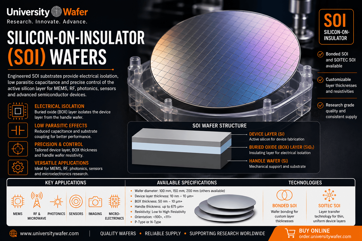
Understanding SOI Wafer Structure
A typical SOI substrate contains three primary layers, each serving a different function in semiconductor fabrication:
- Device Layer: The upper crystalline silicon layer where electronic, photonic, MEMS, or other structures can be fabricated.
- Buried Oxide (BOX) Layer: A silicon dioxide layer that electrically and physically separates the device silicon from the underlying handle wafer.
- Handle Wafer: The thicker silicon substrate that provides mechanical support for the complete SOI structure.
The thickness of each layer can be important to device performance. Researchers should therefore consider device-layer thickness, BOX thickness, handle thickness, resistivity, crystal orientation, and wafer diameter when selecting an SOI substrate.
Why Use Silicon-on-Insulator?
The buried oxide layer distinguishes SOI from conventional bulk silicon wafers . The BOX layer provides electrical isolation between the active silicon device region and the handle substrate, which can be advantageous for specialized electronic and microsystem designs.
SOI substrates also provide a well-defined silicon device layer that can be selected according to the dimensional requirements of a research project. This makes SOI useful for applications where researchers need precise control over the thickness of the active silicon region.
Bonded SOI Wafers
Bonded SOI wafers can be manufactured by joining oxidized and silicon wafer surfaces and subsequently processing the structure to obtain the desired device-layer thickness. Wafer bonding provides flexibility for producing SOI substrates with device and buried oxide dimensions tailored to specialized research applications.
Bonded SOI is particularly useful when researchers require device layers that differ from those commonly available in standard semiconductor production material.
SOI Wafers for MEMS
One of the most important research applications for SOI is MEMS fabrication . The silicon device layer can provide the structural material for microscopic mechanical components, while the buried oxide can serve as an insulating layer or processing boundary.
SOI substrates are used in research involving accelerometers, pressure sensors, resonators, microfluidic structures, microactuators, inertial devices, and other microelectromechanical systems.
SOI for Silicon Photonics
SOI is also an important substrate platform for silicon photonics . The refractive-index contrast between silicon and silicon dioxide allows researchers to fabricate optical structures that guide and manipulate light at microscopic dimensions.
SOI substrates can support research involving optical waveguides, modulators, resonators, photonic integrated circuits, optical sensors, and other silicon-based photonic structures.
RF and High-Resistivity SOI
SOI technology is also studied for RF and microwave devices. Depending on the application, researchers may require high-resistivity silicon handle substrates or specialized SOI structures designed to reduce unwanted substrate-related electrical effects.
When selecting an SOI wafer for RF research, specifications such as handle-wafer resistivity, BOX thickness, device-layer properties, and overall wafer geometry should be considered together with the intended device architecture.
SOI for Sensors and Microdevices
The controlled device-layer thickness and insulating BOX layer make SOI useful for a variety of sensor technologies. Researchers can fabricate microscopic structures directly into the device silicon while using the underlying oxide as part of the fabrication process.
Potential research applications include pressure sensors, inertial sensors, optical sensors, resonators, microheaters, lab-on-chip structures, and other silicon-based microsystems.
Device Layer Thickness
The SOI device layer is one of the most important specifications when selecting a substrate. Thin device layers may be required for electronic and photonic structures, while thicker device layers can be useful for MEMS and other applications requiring greater structural depth.
Researchers should specify the required device-layer thickness and tolerance when requesting SOI wafers, especially when the silicon layer will determine a critical device dimension.
Buried Oxide (BOX) Thickness
The buried oxide layer provides insulation between the device silicon and handle wafer. BOX thickness can influence electrical isolation, optical behavior, thermal characteristics, and fabrication processes.
Researchers requiring silicon dioxide for other semiconductor applications can also explore thermal oxide silicon wafers for thin-film, dielectric, MEMS, and semiconductor research.
SOI Wafer Specifications
When requesting Silicon-on-Insulator wafers, researchers should provide as much information as possible about the required substrate. Important specifications can include:
- Wafer diameter
- Device-layer thickness
- Device-layer thickness tolerance
- Buried oxide (BOX) thickness
- Handle-wafer thickness
- Crystal orientation
- P-type or N-type conductivity
- Device-layer resistivity
- Handle-wafer resistivity
- Surface finish
- Total thickness variation (TTV)
- Quantity required
SOI Wafers for Research and Device Fabrication
UniversityWafer supplies SOI substrates for universities, research laboratories, semiconductor companies, and device developers. Available material can support projects involving MEMS, silicon photonics, RF electronics, sensors, microfabrication, semiconductor devices, and advanced materials research.
Researchers looking for other engineered silicon substrates can also explore silicon epitaxial wafers and silicon-on-sapphire substrates for specialized semiconductor applications.
Get Your Silicon-on-Insulator (SOI) Wafer Quote FAST! Or, buy online and start researching today!
SOI Wafer Technology, Properties and Applications
Silicon-on-Insulator (SOI) technology provides a versatile platform for fabricating electronic, mechanical, optical, and sensing devices. Unlike conventional bulk silicon wafers , SOI substrates contain a buried insulating layer that separates the active silicon device layer from the underlying handle wafer.
This engineered structure allows researchers to select the silicon device layer, buried oxide (BOX), handle substrate, resistivity, orientation, and other parameters according to the requirements of a specific fabrication process.
How Are SOI Wafers Manufactured?
Several manufacturing approaches can be used to produce Silicon-on-Insulator wafers. Wafer bonding is an important method in which silicon and oxidized wafer surfaces are joined to form an SOI structure. Subsequent processing can be used to establish the required device-layer thickness.
Layer-transfer technologies can also be used to produce thin, uniform crystalline silicon device layers over a buried oxide. The appropriate SOI technology depends on factors such as device-layer thickness, uniformity, wafer diameter, electrical requirements, and intended application.
Bonded SOI Wafers
Bonded SOI wafers provide considerable flexibility when researchers require specialized layer thicknesses or substrate configurations. A bonded structure typically combines a silicon device wafer with an oxidized handle wafer, producing the characteristic silicon / BOX / silicon stack.
Bonded SOI substrates are particularly useful for MEMS research , sensors, microfabrication, and applications requiring relatively thick or customized device layers.
SOITEC and Layer-Transfer SOI
Commercial SOI material may also be produced using advanced layer-transfer processes designed to create thin and uniform crystalline silicon layers. These wafers are widely used when precise control of the active silicon thickness is important.
UniversityWafer supplies a variety of SOI material, including bonded and SOITEC-origin substrates, depending on available inventory and required specifications.
Device Layer, BOX and Handle Wafer
An SOI wafer can be understood as three functional layers:
- Device Silicon: The upper crystalline silicon layer used to fabricate devices and structures.
- BOX: The buried SiO2 layer that separates the device layer from the handle substrate.
- Handle Silicon: The thicker supporting wafer that provides mechanical stability.
Each layer can affect device fabrication and performance. For this reason, SOI should be specified as a complete multilayer substrate rather than only by wafer diameter.
Thin vs. Thick SOI Device Layers
The required SOI device-layer thickness varies considerably by application. Thin silicon device layers can be useful for electronic and photonic structures, while thicker device layers are frequently required when the silicon itself forms a mechanical component.
For MEMS fabrication , device-layer thickness can directly determine the height or thickness of fabricated structures such as beams, membranes, resonators, and proof masses.
Buried Oxide (BOX) Layer
The buried oxide layer is generally composed of silicon dioxide and provides electrical isolation between the device silicon and handle substrate. Depending on the application, BOX thickness can also influence optical confinement, thermal behavior, capacitance, and fabrication strategy.
Researchers investigating silicon dioxide independently of an SOI structure can also use thermal oxide silicon wafers with controlled oxide layers.
SOI Wafers for MEMS Fabrication
SOI MEMS wafers are widely used because the device silicon provides a precisely defined structural layer and the buried oxide can function as an etch-stop, sacrificial, or isolation layer depending on the fabrication process.
Potential SOI MEMS applications include:
- Accelerometers
- Gyroscopes and inertial sensors
- Pressure sensors
- Microphones
- Resonators
- Microactuators
- Microfluidic structures
- Optical MEMS
SOI for Silicon Photonics
Silicon photonics is another major research area for SOI substrates. Silicon and silicon dioxide have significantly different refractive indices, enabling optical confinement within patterned silicon structures.
SOI can therefore provide a platform for fabricating optical waveguides, resonators, modulators, couplers, photonic integrated circuits, and optical sensing structures.
High-Resistivity SOI for RF Research
High-resistivity SOI wafers can be useful for RF and microwave research where substrate electrical properties influence device performance. Specialized handle substrates can help researchers investigate reduced substrate losses, improved isolation, and integration of RF structures.
RF SOI research may involve switches, filters, front-end components, microwave circuits, sensors, and other high-frequency semiconductor devices.
SOI for Semiconductor Devices
The electrical isolation provided by the buried oxide makes SOI an important research platform for specialized semiconductor devices. Device structures can be fabricated within the upper crystalline silicon layer while remaining electrically isolated from the bulk handle substrate.
Researchers comparing SOI with other engineered silicon platforms may also consider silicon epitaxial wafers for applications requiring a controlled epitaxial silicon layer without a buried oxide.
SOI Wafer Crystal Orientation
Crystal orientation is another important SOI specification. Common silicon orientations include <100> and <111>, although availability depends on the required SOI configuration.
Orientation can affect etching behavior, mechanical properties, surface processing, and device fabrication. This can be especially important for MEMS processes that use orientation-dependent silicon etching.
SOI Resistivity and Conductivity
Researchers should consider the electrical properties of both the device layer and handle wafer. Depending on the project, SOI substrates may require P-type or N-type silicon and a specified resistivity range.
High-resistivity material may be desirable for RF, microwave, detector, or specialized sensor applications, while other semiconductor processes may require controlled doping within the device silicon.
SOI Wafer Surface Quality
The device surface should be appropriate for subsequent lithography, deposition, etching, bonding, and characterization. Smooth polished silicon surfaces are particularly important when the fabrication process contains nanoscale structures or very thin deposited films.
Researchers requiring extremely smooth silicon surfaces can also explore low surface roughness silicon wafers for AFM, thin-film, bonding, and nanotechnology research.
Characterizing SOI Wafers
SOI substrates can be characterized using several techniques depending on the properties being investigated:
- Ellipsometry: device and oxide layer characterization
- Reflectometry: thin-film and layer-thickness measurements
- AFM: nanoscale surface roughness and morphology
- SEM: fabricated structures and cross-sectional analysis
- Profilometry: step height and surface measurements
- Electrical measurements: resistivity and device-layer properties
For nanoscale surface characterization, researchers can use silicon wafers for Atomic Force Microscopy (AFM) as reference or experimental substrates.
Important SOI Specifications
Before ordering an SOI wafer, consider providing the following information:
- Wafer diameter
- Device-layer thickness and tolerance
- Buried oxide (BOX) thickness
- Handle-wafer thickness
- Device-layer crystal orientation
- Device-layer conductivity and resistivity
- Handle-wafer conductivity and resistivity
- Surface finish
- Total thickness variation (TTV)
- Bow and warp requirements
- Bonded or other SOI technology requirements
- Quantity required
SOI Substrates for Advanced Research
The combination of crystalline silicon, buried oxide, and a mechanically stable handle substrate makes SOI useful across MEMS, RF electronics, silicon photonics, sensors, semiconductor devices, microfabrication, and advanced materials research.
UniversityWafer supplies Silicon-on-Insulator substrates in a wide range of configurations, allowing researchers to select the device layer, BOX layer, handle substrate, orientation, resistivity, and wafer dimensions appropriate for their project.