
Get Your Thermal Oxide Wafer Quote FAST!
UniversityWafer, Inc. supplies thermal oxide silicon wafers for semiconductor research, MEMS, microfabrication, photonics, dielectric studies, thin-film deposition and materials science.
Tell us your required wafer diameter, silicon type, crystal orientation, resistivity, oxide thickness, wet or dry oxidation, surface finish and quantity so we can help identify suitable wafers for your project.
Or, Buy Thermal Oxide Wafers Online and Start Researching Today!
Why Use Thermal Oxide Silicon Wafers?
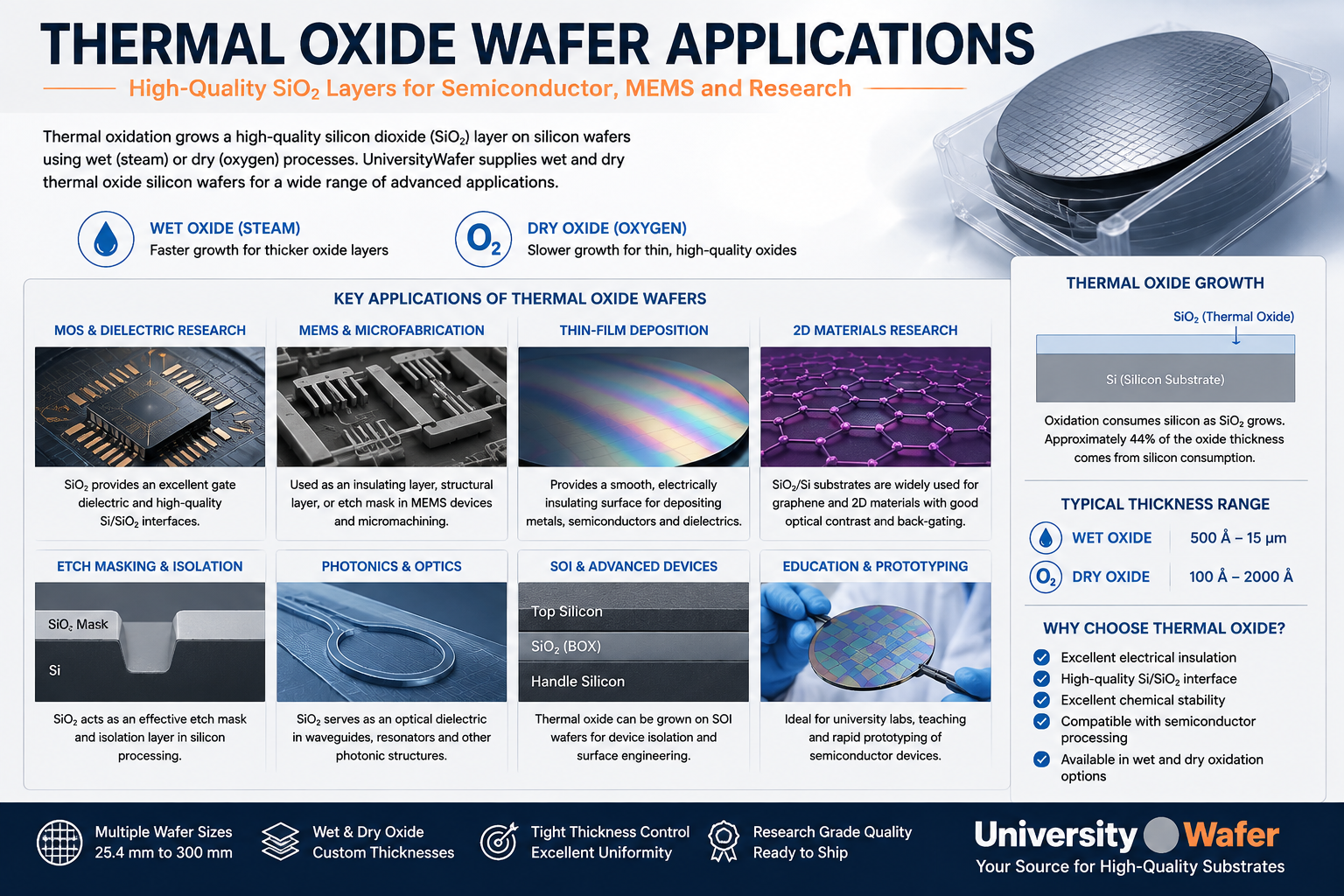
Thermal oxidation creates a silicon dioxide (SiO2) layer by reacting the surface of a silicon wafer with an oxidizing species at elevated temperature. The resulting oxide is not simply deposited on top of the wafer; part of the underlying silicon is consumed as SiO2 forms.
The silicon/thermal-oxide system is fundamental to semiconductor technology because SiO2 is electrically insulating and can form a high-quality interface with crystalline silicon.
Researchers use oxidized silicon wafers as starting substrates for electrical characterization, MOS structures, MEMS, surface studies, thin-film deposition, 2D materials, photonics and microfabrication.
Choosing an Oxide Thickness
The appropriate SiO2 thickness depends on what the oxide must do in the experiment. There is no single oxide thickness that is best for every application.
Thin Thermal Oxide
Relatively thin oxide films are useful when researchers require controlled dielectric thickness or a high-quality Si/SiO2 interface. Dry oxidation is commonly selected for thinner oxides because of its slower growth rate and good film and interface quality.
Applications can include MOS structures, electrical characterization, interface research and other semiconductor experiments.
Thicker Thermal Oxide
Thicker SiO2 layers may be selected for electrical isolation, process masking, MEMS structures, surface modification or experiments requiring a thicker dielectric layer.
Wet oxidation is generally preferred when thicker oxide is needed because water vapor produces a much faster thermal oxidation rate than dry oxygen under comparable processing conditions.
Silicon Is Consumed During Thermal Oxidation
An important feature of thermal oxidation is that the SiO2 layer grows partly into the original silicon surface and partly above it.
As a useful approximation, forming a thermal oxide consumes silicon equal to about 44% of the final SiO2 thickness.
For example, growing approximately 1 µm of thermal oxide consumes roughly 0.44 µm of silicon. This should be considered when precise silicon dimensions or thin device layers are important.
Thermal Oxide for MOS Research
The Si/SiO2 interface has played a central role in metal-oxide-semiconductor technology. Thermal oxide wafers are therefore useful research substrates for studying dielectric behavior, interface properties, capacitance and semiconductor device structures.
For electrically sensitive experiments, researchers should specify the required silicon conductivity type, resistivity, crystal orientation and oxide thickness rather than selecting the oxide thickness alone.
SiO2/Si Substrates for 2D Materials
Oxidized silicon wafers are widely used as substrates for graphene and other two-dimensional materials. The SiO2 surface provides electrical isolation from the underlying silicon, while the silicon can also serve as a global back-gate electrode in suitable device structures.
Certain SiO2 thicknesses are also popular for optical microscopy because thin flakes can produce useful optical contrast against the SiO2/Si substrate. The best thickness depends on the material, illumination and optical system.
Learn more about graphene research substrates .
Thermal Oxide for Thin-Film Research
Thermal oxide silicon wafers provide a smooth, electrically insulating surface for depositing and studying additional materials. Researchers can deposit metals, semiconductors, dielectrics, polymers and other thin films onto SiO2/Si substrates.
This makes oxidized silicon useful as a standardized experimental platform for thin-film deposition , materials characterization and device development.
Thermal Oxide for MEMS and Microfabrication
In MEMS and silicon microfabrication, thermal SiO2 may function as an electrical insulator, surface layer, process mask or part of a multilayer device structure.
When SiO2 is used as an etch mask, the required oxide thickness depends on the etchant, process conditions, oxide-to-silicon selectivity and required silicon etch depth. A thicker oxide does not automatically guarantee adequate masking for every etch process.
Explore MEMS silicon wafers for additional fabrication applications.
Thermal Oxide on SOI
Thermal oxidation can also be performed on exposed silicon surfaces of Silicon-on-Insulator (SOI) wafers for selected research and fabrication processes.
This requires additional attention when the SOI device layer is thin because thermal oxidation consumes silicon. The starting device-layer thickness, target oxide thickness and desired final silicon thickness should therefore be considered together.
Researchers should also distinguish the thermally grown surface oxide from the buried oxide (BOX) already present inside an SOI wafer.
Thermal Oxide vs. Native Oxide
Silicon exposed to air naturally develops a very thin native oxide. This should not be confused with a deliberately grown thermal oxide layer.
Thermal oxidation is performed under controlled processing conditions to produce a specified SiO2 thickness and more reproducible material properties for semiconductor fabrication and research.
What Should You Specify When Ordering?
Oxide thickness is only one part of a thermal oxide wafer specification. For reproducible research, the starting silicon substrate can be equally important.
Include the following whenever possible:
- Wafer diameter
- Silicon crystal orientation: (100), (111), etc.
- Conductivity type: P-type or N-type
- Resistivity range
- Wafer thickness
- Surface finish: SSP or DSP
- Oxidation method: Wet or dry
- Target SiO2 thickness
- Oxide thickness tolerance
- One-side or double-side oxide requirement
- Quantity
If your experiment has critical requirements for oxide uniformity, wafer flatness, surface condition or electrical properties, include those specifications with your request as well.
Need a Custom Thermal Oxide Wafer?
UniversityWafer, Inc. can help researchers source oxidized silicon substrates according to the requirements of their experiment. Available options may vary by wafer diameter, starting silicon specification, target oxide thickness and quantity.
Send us your required silicon specifications, wet or dry oxidation, target SiO2 thickness and quantity for a quote.
Wet and Dry Thermal Oxide Silicon Wafers
UniversityWafer, Inc. supplies thermal oxide silicon wafers for semiconductor fabrication, MEMS, microelectronics, photonics, materials research and university laboratories. Thermal oxidation forms a silicon dioxide (SiO2) layer by exposing silicon to an oxidizing atmosphere at elevated temperature.
Unlike deposited SiO2 films, thermal oxide is formed by consuming part of the silicon surface as the oxide grows. This produces a high-quality Si/SiO2 interface that is valuable for many semiconductor and research applications.
Both wet oxidation and dry oxidation are available depending on the required oxide thickness, growth rate and application.
What Is Thermal Oxide?
Thermal oxide is silicon dioxide grown directly on a silicon surface at elevated temperature. During oxidation, oxidizing species diffuse through the existing oxide and react with silicon at the Si/SiO2 interface, causing the oxide layer to increase in thickness.
Two common oxidation processes are:
- Dry oxidation: uses molecular oxygen (O2) and generally provides slower, more controlled oxide growth.
- Wet oxidation: uses water vapor (steam) and generally provides a substantially faster growth rate, making it useful for thicker oxide films.
Wet vs. Dry Thermal Oxide
| Property | Dry Oxide | Wet Oxide |
|---|---|---|
| Oxidant | Oxygen (O2) | Water vapor / steam (H2O) |
| Growth Rate | Slower | Faster |
| Typical Use | Thin, high-quality oxide layers | Thicker oxide layers |
| Thickness Control | Well suited to thin-film control | Efficient for growing thicker films |
| Electrical Quality | Generally preferred when high dielectric and interface quality are important | Commonly used when rapid growth and greater oxide thickness are more important |
| Common Applications | MOS research, dielectric layers, surface passivation and interface studies | Isolation, masking, MEMS, protective oxide and thicker SiO2 structures |
Wet Thermal Oxide Specifications
Wet thermal oxidation uses water vapor as the oxidizing species. Because wet oxidation grows SiO2 significantly faster than dry oxidation under comparable conditions, it is commonly selected when a relatively thick oxide layer is required.
Typical available wet oxide specifications include:
- Oxide thickness: 500Å to 15 µm
- Target thickness tolerance: approximately ±5%
- Within-wafer uniformity: ±3% or better, depending on specification
- Common wafer diameters: 50mm, 100mm, 125mm, 150mm and 200mm
- Substrate: Silicon; SOI structures may also be available depending on the requested process
- Oxidizing species: Water vapor / steam
Custom oxide thicknesses, wafer diameters and substrate specifications may be available depending on quantity and process requirements.
Dry Thermal Oxide Specifications
Dry thermal oxidation uses oxygen to grow SiO2 on silicon. Its slower growth rate provides useful control for relatively thin oxide layers and it is commonly chosen when oxide and interface quality are important to the experiment.
Typical available dry oxide specifications include:
- Oxide thickness: approximately 100Å to 2,000Å
- 100Å target: approximately ±15Å
- 200Å target: approximately ±20Å
- Above 200Å: approximately ±5% target tolerance
- Within-wafer uniformity: ±3% or better, depending on specification
- Common wafer diameters: 50mm, 100mm, 125mm, 150mm and 200mm
- Substrate: Silicon; SOI structures may also be available depending on the requested process
- Oxidizing species: Oxygen (O2)
How Thermal Oxide Grows on Silicon
Thermal oxidation does not simply deposit SiO2 onto the wafer. Oxygen-containing species reach the silicon interface and react with the underlying silicon to form additional silicon dioxide.
As a useful rule of thumb, growing thermal SiO2 consumes approximately 0.44 times the final oxide thickness in silicon. The remainder of the oxide thickness extends above the original silicon surface.
This distinction can matter in MEMS, microfabrication and other applications where dimensional control is important.
Single-Side vs. Double-Side Thermal Oxide
Standard furnace oxidation can oxidize exposed silicon surfaces on both sides of a wafer. If an application requires oxide on only one surface, additional masking or process steps may be necessary to protect or remove oxide from the opposite side.
When requesting a quote, specify whether your project requires oxide on both sides, oxide on one side, or a particular backside condition.
Thermal Oxide Wafer Applications
Thermal SiO2 is one of the most widely studied dielectric materials in silicon technology. Oxidized silicon wafers are useful as starting substrates and reference materials for a broad range of research and fabrication processes.
MEMS and Microfabrication
Thermal oxide can serve as an insulating layer, surface layer, masking material or part of a multilayer structure in MEMS fabrication and silicon micromachining.
MOS and Dielectric Research
High-quality Si/SiO2 interfaces make thermal oxide silicon wafers useful for MOS structures, dielectric characterization, interface studies, electrical measurements and semiconductor education.
Thin-Film Deposition
Oxidized silicon provides an electrically insulating and well-defined surface for depositing metals, semiconductors, polymers and other thin films.
Thermal oxide wafers are therefore frequently used as experimental substrates for materials science, nanotechnology and device research.
Optical and Photonics Research
SiO2 can function as an optical dielectric and as part of silicon-based photonic structures. Researchers may select a specific oxide thickness according to the optical design, wavelength or device architecture.
Graphene and 2D Materials Research
SiO2/Si substrates are widely used in graphene and other two-dimensional-material research. The oxide provides an insulating surface, while selected oxide thicknesses can improve optical contrast for locating thin flakes under an optical microscope.
Etch Masking and Process Development
Thermal SiO2 can be used as a masking material in selected silicon etching processes because silicon dioxide and silicon can exhibit different etch rates. Required oxide thickness depends on the etch chemistry, selectivity and target etch depth.
Thermal Oxide on SOI Wafers
Thermal oxidation can also be incorporated into selected Silicon-on-Insulator (SOI) structures.
Because oxidation consumes silicon, the required final device-layer thickness should be considered when oxidizing thin SOI device layers. Researchers should specify whether the requested thickness refers to the silicon layer before or after oxidation.
Thermal Oxide vs. Deposited SiO2
Thermal oxide should not be confused with deposited silicon dioxide. Thermal SiO2 is produced by oxidizing the silicon substrate itself, whereas deposited SiO2 is added to a surface using a deposition process such as CVD, PECVD or TEOS-based processing.
Deposited oxide can be useful when thermal oxidation is unsuitable or when oxide must be formed over materials other than silicon. The appropriate process depends on temperature limits, film thickness, interface requirements and device design.
How to Specify Thermal Oxide Wafers
When requesting thermal oxide wafers, provide as much information as possible about both the starting silicon substrate and the required SiO2 film.
Useful specifications include:
- Wafer diameter
- Silicon crystal orientation, such as (100) or (111)
- P-type, N-type or intrinsic/undoped requirement
- Resistivity range
- Wafer thickness
- Single-side or double-side polished substrate
- Wet or dry thermal oxidation
- Target oxide thickness
- Oxide thickness tolerance and uniformity
- One-side or double-side oxide requirement
- Quantity
Order Thermal Oxide Silicon Wafers
UniversityWafer, Inc. supplies thermal oxide silicon substrates for university laboratories, semiconductor development, MEMS, materials science, photonics and other research applications.
Whether your experiment requires a thin dry oxide for interface studies or a thicker wet oxide for isolation, masking or fabrication research, send us your required wafer diameter, silicon specifications, oxide thickness, oxidation method and quantity.
Get Your Thermal Oxide Wafer Quote FAST! Or, Buy Wafers Online »
Related Thermal Oxide & Silicon Wafer Resources
- Thermal Oxide Deposition – Learn about growing silicon dioxide layers on silicon wafers for semiconductor research and fabrication.
- Silicon Wafers – Browse silicon substrates available in different diameters, orientations, resistivities and surface finishes.
- Silicon-on-Insulator (SOI) Wafers – Explore SOI substrates for MEMS, photonics and advanced semiconductor device research.
- TEOS Oxide – Learn about deposited SiO2 films produced using TEOS-based processes as an alternative to thermal oxidation.
- Chemical Vapor Deposition (CVD) – Explore CVD processes used to deposit dielectric, semiconductor and other thin films.
- Thin-Film Deposition – Learn about thin-film materials and deposition techniques used in semiconductor and materials research.
- MEMS Wafers – Explore silicon substrates used for MEMS fabrication, micromachining and sensor research.
- Silicon Nitride Wafers – Compare Si3N4-coated substrates with SiO2 wafers for dielectric, masking and microfabrication applications.