
Single Crystal Indium Phosphide Wafers (InP)
Indium Phosphide wafers 2" and 3" available in Test and Prime grades. Custom orders always accepted. Small quantities is our specialty
Get Your Float Zone Silicon Wafer Quote FAST! Or, Buy Online and Start Researching Today!
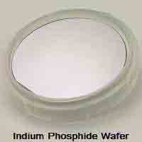
Typical 50.8mm Diameter InP Wafer

Other Wafers Include
- Aluminum Wafers
- Germanium (electrical and optical Grades)
- Graphene
- LiNbO3
- LiTaO3
- Silicon on Insulator
- Silicon on Sapphire
- GaN/AlN on Sapphire
- InGaAs
Below are some of InP wafer applications
- Fiber optics network components
- Dense wavelength division multiplexing (DWDM) lasers
- Vertical-Cavity Surface-Emitting Laser (VCSEL)
- Pump Lasers
- PIN and APD diodes
- Amplifiers
- For high speed electronics circuit using HBT
- HEMT for fiber optics, wireless and space communication and automotive applications.
 Order InP Wafers and Other Substrates Online!
InP Wafers are used in telecommunications and microelectronics fields where high power small devices are required.
"'wet chemistry' photodetectors are up to 10 times more sensitive to infrared light than those made with conventional methods, where a single crystal of indium phosphide (InP) serves as a platform for the growth of subsequent crystals, one on top of another."
Indium Phosphide Photodetectors
 Indium phosphide is used by companies such as Infinera to manufacture photonic integrated circuits for the optical and telecommunications industries, enabling wavelength splitting and multiplexing applications (8). As an ideal candidate for use in photodetectors and modulators, indium phosphide (InP) can be used to produce efficient and laser-sensitive photodsector modulators at wavelengths outside the typically used window. In view of the low energy barrier between the base - doped n and the laser - a large hole current is injected into the n-doped base when the energy barriers are lowered and photons generated by the electrons are injected to mitigate the effect of the space charge. [Sources: 2, 7, 10]
This coefficient depends on the electric field applied to the material; for example, at 240 kV / cm, the electron-hole ratio is 50: 1. In this context, the pn compound tends to produce photons from the active layer whose energy corresponds to the band gap in the materials from which the photons originate. The generation rate can be calculated by assuming that each absorbed photon produces an electron / hole pair. As the optical field propagates through the device, light is absorbed at the speed of one photon per electron and one hole per electron. [Sources: 4, 5, 7]
It is also apparent that there is a tendency in this region to make InP a poor choice for propagation, making it unsuitable for use as a photodiode in photodiodes or as an optical fiber. It would be highly desirable to have an APD that can convert light into electricity without multiplication and is therefore a suitable candidate for the use of fibre optics. InCarrier layer 5 may also affect the performance of the sensor integrated into the photodicode field, but has the advantage of having a single integrated structure that would provide a demultiplexing capability to detect the separate wavelengths present in optical fibers. [Sources: 4, 5, 8]
Since both components are photovoltaics and react to light at inverted voltages, the connection between the P and the I photodiode must cross the entire field of the control layer and be in the ingaas. Therefore, we have a conventional transistor scale that leads to an extremely high t, even though most incident photons are not absorbed. [Sources: 2, 6]
The device in Jackson uses several semiconductor elements that are connected in series from an electrical point of view. The incoming radiation is coupled with the first element in a tandem arrangement of elements, whereby the element with the largest band gap is placed first in the row between the elements. This type of strip alignment can minimize the accumulation of absorption, collection and strip discontinuities, which are discussed in detail in Section 4. P-type absorber layer, it can provide a high excess energy for the injected electrons in both the InP and collector layer. [Sources: 5, 7]
The material with the best absorption has no high ionization coefficient, and the materials with the best absorption do not have the desired optical region. A material such as silicon, which has a band spacing of less than 1.5 micrometers (0.1 nm), not only does this happen, but the low noise gain in this region will also have an impact on the absorption of the incident radiation, resulting in lower noise and amplification. Since silicon is a semiconductor with a very high band gap (also called multiplication), it has indirect band gaps, making it a poor absorption material. [Sources: 4]
As mentioned above, the P-type InP materials are completely transparent to the radiation in the wavelength range of the photodiodes, while the p-Ingaas materials are very absorbent. Likewise, they can be completely opaque to radiation, as it is stated below. As mentioned above, photodiodes are used in the wavelength range, which strongly absorbs the in-p ingCarbon material. [Sources: 1, 9]
Indium gallium arsenide (InGaAs) is particularly suitable as it has a relatively short absorption length and therefore operates in the wavelength range of the photodiodes, in which the absorbing layer can be easily caught by the photocarrier. The detecting active layer, consisting of ingas material, can have an adjustable band gap depending on its composition of In GaAs, depending on the absorption wavelength and the thickness of its layer. [Sources: 3, 8]
Indium phosphide (InP) is preferred to InGaAs because it has a higher band gap energy than In GaAs and can be used in photodiodes (citation required), but it is also preferred to InGalliumAs because it has large band gaps and the energy of IngaAs. [Sources: 4, 10]
Gentec Electro-Optics offers a power detector based on silicon germanium photodiodes with a power output of up to 750 mW. This achieves the required bandgap combination of InGaAs and InGalliumAs with a bandgap energy of 1.5 - 2.0 mG / s. [Sources: 3, 10]
The optical properties of the photodetector can be simulated with the Q-2 layer of InGaAs and InGalliumAs as well as the q-3 layer. The longer wavelength section curve corresponds roughly to the band gap energy of each layer determined by photoluminescence. We can calculate the optical absorbed power and define the external quantum efficiency (EEP), which is the ratio of unamplified electrons to incident photons. The quantum efficiency of a photodiode is a measure of how much incident and absorbed photons in the form of photons - to - electrons (Q - E ratio) contribute to photocurrents. The absorption that occurs in Q / 2 layers is the absorption of photons by the In GaAs layer, and the longer the wavelength of the absorption, the greater the quantum efficiency of this layer and the higher the power output. [Sources: 0, 2, 3, 5]
Sources:
[0]: https://support.lumerical.com/hc/en-us/articles/360042332014-InP-InGaAs-uni-traveling-carrier-photodetector
[1]: https://www.google.com.gi/patents/US4999696
[2]: https://www.nature.com/articles/srep33368
[3]: https://www.rp-photonics.com/photodiodes.html
[4]: https://patents.google.com/patent/US6147391
[5]: https://www.google.com.pg/patents/US4213138
[6]: https://www.google.com/patents/US6555890
[7]: https://www.spiedigitallibrary.org/conference-proceedings-of-spie/11354/2555021/High-performance-waveguide-unitraveling-carrier-photodetector-based-on-GaAs05Sb05-InP/10.1117/12.2555021.full
[8]: https://patents.justia.com/patent/9018727
[9]: https://www.google.si/patents/US4904608
[10]: https://en.wikipedia.org/wiki/Indium_phosphide