I dont have precise requirements for these specifications. I’ll glue the chips to silicon wafers for etch tests anyway. It would be cool to have 4 inch wafers as carriers for etching tests, to see how an etching process would behave on a full wafer. Quote: 10 wafers optical grade, X Cut.
Lithium Tantalate (LiTaO3) for Research and Production
100mm LiTaO3 Substrates Used for Etching Tests
An associate professor researching Si3N4-based nonlinear integrated photonics requested the following quote:
Reference #304096 for specs and pricing.
Get Your FAST! Or, Buy Online and Start Researching Today!
Lithium Tantalate (LiTaO3) Wafers in stock:
- LiTaO3 optical grade, X-cut, 10x10x0.5mm, DSP
- LiTaO3 saw grade, X-cut, 10x10x0.5mm, SSP
- LiTaO3 saw grade, X-cut, 3" Dia x 0.5mm wafer, SSP
- LiTaO3 optical grade, Y-cut, 10x10x0.5 mm, DSP
- LiTaO3 saw grade, Y-cut, 10x10x0.5mm, SSP
- LiTaO3 Saw grade, Y-cut wafer with 128 degree off , 3" dia x0.5 mm , SSP-1
- LiTaO3 Saw grade, Y-cut wafer with 36 degree off , 2" dia x0.5 mm , SSP-1
- LiTaO3 Saw grade, Y-cut wafer with 36 degree off , 3" dia x0.4 mm , SSP
- LiTaO3 Saw grade, Y-cut wafer with 36 degree off , 4" dia x0.35 mm , SSP
- LiTaO3 Saw grade, Z-cut, 10x10x0.5 mm, SSP
- LiTaO3 optical grade, Z-cut, 10x10x0.25 mm, DSP
- LiTaO3 optical grade, Z-cut, 10x10x0.5 mm, DSP
- LiTaO3 optical grade, Z-cut, 10x10x1.0 mm, DSP
- LiTaO3 optical grade, Z-cut wafer, 2" Dia x 0.5mm , DSP
- LiTaO3 optical grade, Z-cut wafer, 3" Dia x 0.5mm , DSP
- LiTaO3 saw grade, Z-cut, 3"Dia x0.5mm wafer, SSP
🧪 Lithium Tantalate (LiTaO₃) Wafers for Photonics, SAW, and MEMS Applications
UniversityWafer, Inc. offers high-quality Lithium Tantalate (LiTaO₃) wafers in a variety of orientations, cuts, and specifications for researchers and commercial device manufacturers. LiTaO₃ is widely used in acousto-optic, piezoelectric, and electro-optic applications due to its exceptional crystal and dielectric properties.
🔍 Available Specifications
| Property | Options & Values |
|---|---|
| Orientation | X-cut, Y-cut, Z-cut, 36° Y-cut, 128° Y-cut |
| Diameter | 2", 3", 4", 6" |
| Thickness | 200 µm – 1000 µm |
| Polish | Single or Double Side Polished (SSP/DSP) |
| Surface Roughness | < 1 nm Ra (DSP available for optical-grade applications) |
| Material Type | Congruent or Near-Stoichiometric |
| Resistivity | High-resistivity dielectric substrate |
| Crystal Type | Single-crystal, Y/LT grown |
| Usage | Epi-ready, SAW-ready, optical-quality |
📦 Custom specs available on request – fast lead times and academic discounts offered.
🔬 Key Features of LiTaO₃ Wafers
-
High thermal and mechanical stability
-
Excellent piezoelectric coupling (ideal for SAW/BAW devices)
-
Low dielectric loss and broad optical transmission range
-
Strong nonlinear optical behavior for harmonic generation
-
Ideal for MEMS resonators, electro-optic switches, and IR detectors
⚙️ Common Applications
-
📱 RF Filters: Used in smartphones, 5G, and WiFi SAW/BAW devices.
-
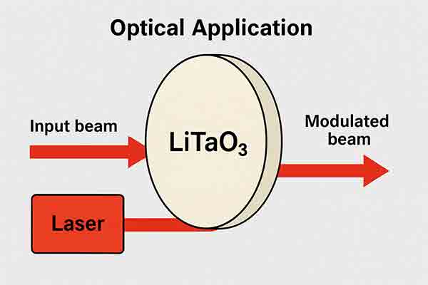
💡 Electro-Optic Modulators: Telecom-grade modulators and Pockels cells.
-
🔁 Frequency Converters: SHG and THG in nonlinear optics.
-
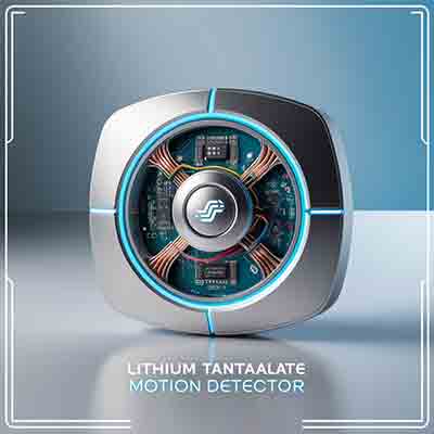
📷 Pyroelectric IR Sensors: Thermal and motion detection.
-
⚙️ MEMS/NEMS: Piezo-actuators, resonators, and gyroscopes.
🏭 Why Order From UniversityWafer, Inc.?
-
✅ ISO and RoHS compliant partner fabs
-
✅ Academic and volume discounts
-
✅ Quick turnaround and global delivery
-
✅ Technical support for device R&D
Lithium Tantalate (LiTaO3) Wafers for Research and Production
LiTaO3 is a perovskite with unique optical properties.
Used in:
- Non-linear Optics
- Passive infrared sensors
- Motion detectors
- Terahertz generation and detection
- Surface acoustic wave applications
- Cell phones
- Pyroelectric nuclear fusion
Please let us know what specs and quantity you would like us to quote?

What are Lithium Tantalate (LiTaO3) Substrates Used For?
Lithium Tantalate (LiTaO₃) is a ferroelectric and piezoelectric single-crystal material that’s widely used in optoelectronic, photonic, and RF (radio frequency) semiconductor devices due to its unique electro-optic, acousto-optic, piezoelectric, and nonlinear optical properties.
🔬 Material Properties of LiTaO₃
| Property | Value / Description |
|---|---|
| Crystal system | Trigonal (R3c space group) |
| Melting point | ~1650 °C |
| Transparency range | 0.25–5.5 µm (UV to mid-IR) |
| Dielectric constant (ε) | ~43 along z-axis |
| Electro-optic coefficient | High (used in modulators and Pockels cells) |
| Piezoelectric coefficient | Strong (used in SAW and BAW filters) |
| Coercive field | Lower than LiNbO₃ (good for stable ferroelectric behavior) |
⚙️ Semiconductor & Device Applications
Lithium Tantalate is not a "semiconductor" in the conventional sense (like silicon or GaN), but it's a critical substrate and functional material in many semiconductor-adjacent technologies.
📡 1. RF Filters (SAW & BAW Devices)
-
SAW (Surface Acoustic Wave) and BAW (Bulk Acoustic Wave) filters for mobile phones, IoT, and 5G.
-
Excellent for high-frequency signal filtering due to low acoustic losses.
-
Z-cut and 36° Y-cut LiTaO₃ are popular in SAW applications.
🔁 2. Electro-Optic Modulators
-
Pockels effect in LiTaO₃ allows high-speed modulation of light.
-
Used in fiber optic telecom and Q-switching in lasers.
💡 3. Nonlinear Optical Devices
-
Used for frequency doubling (e.g., 1064 nm → 532 nm).
-
Less prone to photorefractive damage than LiNbO₃ at higher power levels.
🧠 4. Pyroelectric and Infrared Sensors
-
Converts IR radiation into an electrical signal.
-
Used in motion detectors, thermal cameras, and spectroscopy.
🧬 5. Thin Film Piezoelectric Layers (in MEMS)
-
Used in MEMS actuators, gyroscopes, and sensors.
-
Thin films of LiTaO₃ are being explored for integration on CMOS-compatible platforms.
🔄 Comparison with Lithium Niobate (LiNbO₃)
| Feature | LiTaO₃ | LiNbO₃ |
|---|---|---|
| Electro-optic effect | Lower than LiNbO₃ | Higher |
| Piezoelectricity | Better for SAW due to higher stability | More prone to photorefractive damage |
| Thermal stability | Higher | Lower |
🧩 Common Substrate Forms
-
X-cut, Y-cut, and Z-cut wafers: orientation defines acoustic and optical properties.
-
Standard wafer sizes: 2"–6", polished or double-side polished, epi-ready available.
🛠️ Industry Use Cases
-
Telecom: RF front-end filters in smartphones (especially LiTaO₃ SAW filters).
-
Defense & Aerospace: Optical modulators and IR sensors.
-
Photonics research: Nonlinear optical generation and quantum optics.
-
Consumer electronics: Motion and IR detection in security systems.

