Zinc Selenide (ZnSe) Wafers & Optical Substrates
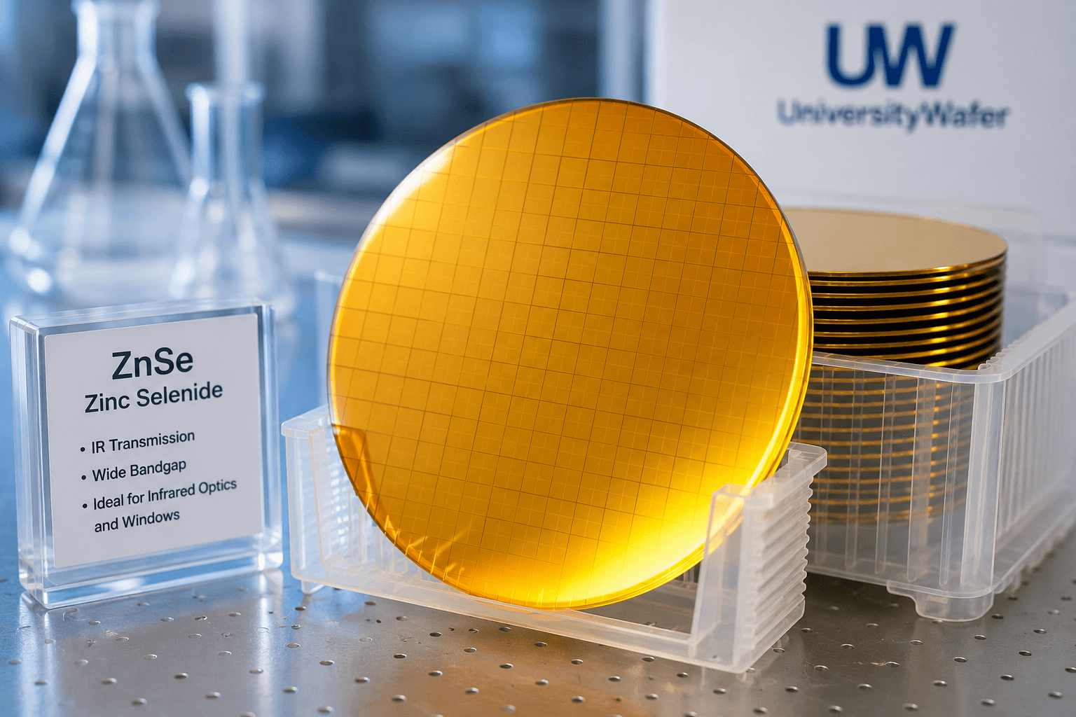
Zinc Selenide (ZnSe) wafers are high-performance II–VI semiconductor substrates prized for their exceptional infrared transparency, wide bandgap, and excellent optical properties. UniversityWafer supplies optical-grade and research-grade ZnSe substrates, crystals, and optical windows with custom diameters, thicknesses, crystal orientations, and polished finishes for CO2 laser optics, FTIR spectroscopy, thermal imaging, photonics, infrared sensors, and advanced semiconductor research.
Get Your Zinc Selenide (ZnSe) Wafer Quote FAST!
UniversityWafer supplies premium-quality Zinc Selenide (ZnSe) wafers,
crystals, optical windows, and custom substrates for universities, national
laboratories, defense contractors, and semiconductor manufacturers worldwide.
ZnSe is a leading II–VI semiconductor valued for its exceptional
infrared transmission, wide bandgap, and excellent optical performance in
research and industrial applications.
Whether you are developing CO2 laser optics,
FTIR spectroscopy systems, infrared imaging components,
photonic devices, optical coatings, or semiconductor research platforms, our
engineering team can supply ZnSe substrates manufactured to your exact
specifications. Standard inventory is available alongside fully customized
solutions for prototype and production projects.
Recent Research Inquiry
"Our laboratory is developing infrared optical components for a mid-wave
infrared imaging system and requires double-side polished Zinc
Selenide (ZnSe) wafers with low surface roughness, custom thickness,
and precise diameter tolerances. Could you provide available orientations,
optical quality specifications, pricing, and lead times for research
quantities?"
Available Zinc Selenide Wafer Specifications
- Single crystal ZnSe wafers and substrates
- Optical-grade and research-grade Zinc Selenide
- Single-side polished (SSP) and double-side polished (DSP)
- Custom diameters, thicknesses, and edge profiles
- Standard and custom crystal orientations
- Laser-quality optical windows and optical blanks
- Diced pieces for device fabrication and laboratory research
- Prototype through high-volume production quantities
Applications
ZnSe substrates are widely used for infrared optics, thermal imaging,
high-power CO2 laser systems, spectroscopy, photonic research,
nonlinear optics, optical coatings, semiconductor device development,
medical imaging, aerospace sensors, and advanced defense technologies.
Simply complete the quotation form with your required wafer diameter,
thickness, orientation, polish, quantity, and any additional specifications.
One of our application engineers will quickly recommend the most suitable
ZnSe substrate for your project and provide competitive pricing.
Get Your Quote FAST! Or,
Buy Online
and Start Researching Today!
What Are Zinc Selenide (ZnSe) Wafers?
Zinc Selenide (ZnSe) is a II–VI semiconductor with a
wide direct bandgap of approximately 2.7 eV, making it an
excellent material for infrared optics, optoelectronics, and photonic
applications. ZnSe offers exceptional transmission from the visible spectrum
into the infrared region, low optical absorption, and excellent resistance to
thermal shock. These properties make ZnSe wafers ideal for high-power laser
systems, infrared imaging, spectroscopy, and advanced semiconductor research.
UniversityWafer supplies ZnSe wafers, substrates, optical windows,
crystals, and diced pieces in standard and custom specifications for
universities, research laboratories, aerospace organizations, and commercial
manufacturers.
Why Researchers Choose ZnSe
| Property |
Benefit |
Typical Applications |
| Wide Bandgap |
Excellent optical transparency with low absorption across visible and infrared wavelengths. |
Infrared optics, photonics, optical coatings. |
| High Infrared Transmission |
Outstanding transmission from approximately 0.5–22 μm. |
CO2 lasers, thermal imaging, FTIR spectroscopy. |
| Low Optical Loss |
Produces high-quality optical components with minimal scattering. |
Laser optics, optical windows, beam delivery systems. |
| Machinability |
Can be fabricated into precision optical components and custom substrates. |
Research optics, infrared sensors, aerospace optics. |
Applications of Zinc Selenide Wafers
ZnSe substrates are widely used throughout optical engineering,
microelectronics, and scientific research due to their excellent optical and
electrical characteristics.
- CO2 laser optics and beam delivery systems
- Infrared optical windows
- Thermal imaging equipment
- FTIR spectroscopy systems
- Infrared detectors
- Photonic integrated devices
- Optical coatings and thin-film research
- Medical laser systems
- Defense and aerospace infrared optics
- Semiconductor and materials science research
Available ZnSe Wafer Specifications
UniversityWafer offers custom Zinc Selenide wafers to meet a
wide variety of research and manufacturing requirements. Available
specifications include:
- Optical-grade and research-grade ZnSe
- Single crystal Zinc Selenide substrates
- Single-side polished (SSP) and double-side polished (DSP)
- Custom wafer diameters and thicknesses
- Precision optical polishing with low surface roughness
- Laser-quality optical windows and blanks
- Diced substrates and custom geometries
- Prototype through production quantities
Custom ZnSe Solutions for Research and Industry
Whether your project requires a precision optical substrate for a
high-power laser, an infrared window for thermal imaging, or a custom
Zinc Selenide wafer for photonic or semiconductor research,
UniversityWafer can manufacture substrates to your exact specifications. Our
engineering team works closely with customers to provide custom dimensions,
surface finishes, crystal orientations, and polishing options while maintaining
the optical quality required for demanding scientific and industrial
applications.
Related Resources
