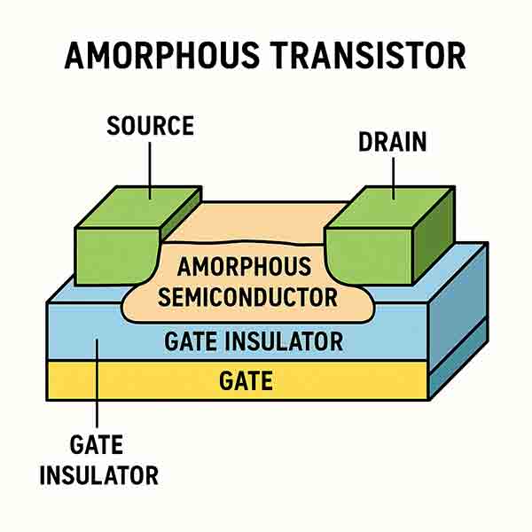
Recommended R&D Substrate for Amorphous Transistor Fabrication
Below are recommended silicon wafer specification tailored for amorphous transistor (TFT) R&D — especially if you're using a-Si:H or IGZO on silicon with thermal oxide:
Get Your Quote FAST! Or, Buy Online and Start Researching Today!
Recommended R&D Substrate for Amorphous Transistor Fabrication
| Parameter | Specification |
|---|---|
| Substrate Type | Silicon Wafer with Thermal Oxide |
| Wafer Diameter | 100 mm (4") or 150 mm (6") |
| Crystal Orientation | ⟨100⟩ |
| Doping Type | Intrinsic (Undoped) or Lightly Doped p-type |
| Resistivity | > 1,000 Ω·cm (high resistivity preferred) |
| Oxide Layer | 300 nm Thermal SiO₂ (dry or wet) |
| Polish | DSP (Double-Side Polished) |
| Grade | Prime |
| Surface Quality | < 1 nm RMS roughness (ideal for thin-film growth) |
| Thickness | ~500–525 µm |
| Flat | SEMI-standard primary flat |
| Application | Acts as gate electrode (Si), gate dielectric (SiO₂), TFT stack deposited on top |
💡 Why this substrate?
-
The high-resistivity Si acts as a back-gate.
-
The thermal oxide (300 nm) serves as a gate dielectric.
-
Perfect for spin coating, PECVD, sputtering, or ALD of active layers.
-
Works well for IGZO, a-Si:H, dielectrics, and metal contacts in a full TFT stack.
Silicon Wafer Specification Sheet
Application: Substrate for Fabrication of Amorphous Transistors (a-Si:H / IGZO TFTs)
| Parameter | Specification |
|---|---|
| Substrate Type | Silicon with Thermal Oxide |
| Wafer Diameter | 100 mm (4 inch) or 150 mm (6 inch) |
| Crystal Orientation | ⟨100⟩ |
| Doping Type | Intrinsic (Undoped) or Lightly Doped p-type |
| Resistivity | > 1,000 Ω·cm |
| Oxide Thickness | 300 nm (Thermal SiO₂) |
| Oxide Type | Dry or Wet Thermal Oxide |
| Wafer Thickness | 500 ± 25 µm |
| Surface Polish | DSP (Double-Side Polished) |
| Wafer Grade | Prime Grade |
| Surface Quality | Roughness < 1 nm RMS |
| Flat Type | SEMI-standard primary flat |
| Packaging | Single wafer cassettes in vacuum-sealed containers |
| Use Case | TFT fabrication with PECVD, sputtering, photolithography, etc. |
✅ Ideal for:
-
Back-gated TFT test structures
-
Gate dielectric research
-
Thin-film deposition studies (a-Si, IGZO, etc.)
-
Transparent/flexible electronics prototyping
What is an AmorphousTransistor?
An amorphous transistor is a type of thin-film transistor (TFT) made using amorphous semiconducting materials, most commonly amorphous silicon (a-Si) or amorphous oxide semiconductors like indium gallium zinc oxide (IGZO).

Key Characteristics:
-
"Amorphous" means the semiconductor lacks long-range crystalline order, unlike crystalline silicon.
-
They are typically deposited at low temperatures (~150–300°C), making them compatible with flexible substrates like plastic or glass.
-
Often used in large-area electronics where performance can be lower but cost and manufacturability are more important.
Applications:
-
Displays: Most commonly used in LCD and OLED displays to control each pixel.
-
Flexible electronics: Ideal for bendy screens and wearable devices due to low-temperature processing.
-
Low-cost sensors and transparent electronics (especially with oxide semiconductors).
Advantages:
-
Low-cost fabrication using vacuum deposition or solution processes.
-
Large-area compatibility, e.g., TV panels or solar cells.
-
Substrate flexibility — works on glass, plastic, or metal foils.
Disadvantages:
-
Lower carrier mobility compared to crystalline or polycrystalline materials.
-
a-Si: ~0.5–1 cm²/V·s
-
IGZO: ~10–20 cm²/V·s
-
-
Instability under prolonged electrical or light stress (especially in a-Si).
Summary:
An amorphous transistor is a cost-effective, low-performance, large-area switch used in devices where ultra-high-speed or high current drive isn’t required. It's a foundational technology for modern flat-panel displays and emerging flexible electronics.
What Silicon Wafer Specs are Requited to Fabricate The Amorphous Transistor?
To fabricate amorphous transistors (typically a-Si:H TFTs or oxide TFTs), the silicon wafer is not the active semiconducting layer, but it may still be used as a support substrate or process carrier during development or prototyping, especially in research or small-scale fabrication.
However, for display or flexible electronics manufacturing, the devices are often built on glass or plastic substrates, not silicon. Still, when silicon wafers are used (especially in lab or prototype settings), here are the typical specifications:
✅ Recommended Silicon Wafer Specs for Amorphous Transistor Fabrication:
| Property | Recommended Spec | Reason |
|---|---|---|
| Material | Monocrystalline Silicon (CZ) | Stable, smooth surface for thin-film deposition |
| Orientation | ⟨100⟩ or ⟨111⟩ | ⟨100⟩ more common; doesn't matter for a-Si:H |
| Diameter | 100 mm or 150 mm (4" or 6") | Standard for R&D and pilot production |
| Type | Intrinsic or Lightly Doped (p-type) | Not used as the active layer; conductivity irrelevant |
| Resistivity | > 1 Ω·cm (high resistivity) | Acts as an inert platform, not involved electrically |
| Polish | DSP (Double-Side Polished) | Ensures flatness and ease of thin-film deposition |
| Surface Roughness | Prime or SEMI-standard <1 nm RMS | Critical for uniform TFT layer deposition |
| Thermal Oxide | Optional (e.g., 100–300 nm SiO₂) | May be used as gate dielectric or insulation |
🧪 Example Use in R&D:
In research environments, amorphous silicon or IGZO layers are often deposited on thermal SiO₂/Si wafers. The silicon acts as a global gate and the oxide as the dielectric, allowing for easy testing of TFT structures before scaling to flexible substrates.
⚠️ Note:
In mass production, silicon wafers are not used for TFTs in displays. Instead:
-
Glass is used for large flat panel TFTs (LCDs, OLEDs).
-
Flexible plastic (PI, PET) is used for bendable electronics.
-
Silicon wafers are only process tools or research substrates.
