Get Your Quote FAST! Or, Buy Online and Start Researching Today!
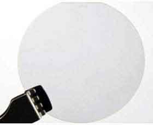
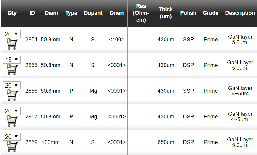
- GaN epitaxial wafers consist of GaN layer on 6H-SiC substrate. 50 mm diam on axis, n-type, GaN thickness ~0.5 um
- GaN layer on sapphire, 50mm diameter on-axis, n-type, GaN thickness 0.5-10 um.
- GaN/AIN/SiC epitaxial wafer consisting of GaN layer on AIN layer on 6H silicon carbide. 50mm in diameter on-axis, n-type. GaN thickness ~(0.5-0.8) um. AIN thickness ~0.1um.
- GaN/AIN/AI2O3 epitaxial wafer consists of GaN layer on AIN layer on sapphire. 50mm in diameter, on-axis, n-type, GaN thickness ~(0.5-0.8) um, AIN thickness ~0.1 um.
Related Wide-Bandgap & Semiconductor Resources
- GaN on Sapphire Substrates
- Gallium Arsenide (GaAs) Wafers
- Silicon Carbide (SiC) Wafers
- Silicon Wafers – Prime & Test Grades
- Compound Semiconductor Substrates
- AlGaN / GaN Heterostructures
- Sapphire (Al₂O₃) Wafers
- Epitaxial Silicon Wafers
- Solar & Power Semiconductor Wafers
- Complete Wafer Products Catalog
What are Gallium Nitride on Sapphire Wafers?
Gallium nitride (GaN) is a type of material that is used to make very small, very fast electronic devices. It is made up of atoms of gallium and nitrogen, and it is very good at conducting electricity and heat.
GaN wafers are very thin slices of GaN material that are used to make tiny electronic devices, like transistors and light-emitting diodes (LEDs). Transistors are like little switches that can turn electronic signals on and off very quickly, and LEDs are tiny light bulbs that can be used to make different colors of light.
GaN wafers are used in a lot of different things, like phones, TVs, and computers. They are also used in special machines that use a lot of electricity, like airplanes and electric cars.
GaN wafers are made using very advanced machines and techniques, and it takes a lot of time and skill to make them. They are very important for a lot of different technologies, and they help make our lives easier and more convenient.
Why GaN Wafers Matter: Key Advantages Over Silicon
Gallium Nitride (GaN) is a wide-bandgap III–V semiconductor that delivers substantial performance advantages compared to traditional silicon wafer, making it a preferred choice for high-power, high-frequency, and high-temperature applications.:contentReference[oaicite:1]{index=1}
- Wide bandgap (~ 3.4 eV): GaN can sustain higher breakdown voltages and high electric fields, enabling devices that operate at high power or high voltage.:contentReference[oaicite:2]{index=2}
- High electron mobility & saturation velocity: Enables fast switching and high-frequency operation — ideal for RF amplifiers, power converters, and high-speed electronics.:contentReference[oaicite:3]{index=3}
- Superior thermal performance: GaN handles high temperatures and high power density better than silicon-based devices, supporting more compact, efficient designs with reduced cooling needs.:contentReference[oaicite:4]{index=4}
- Smaller device footprint & higher power density: Thanks to lower on-resistance and higher breakdown strength, GaN devices and wafers can enable lighter, more compact, and more efficient power and RF systems.:contentReference[oaicite:5]{index=5}
Common Applications of GaN Wafers & Substrates
GaN wafers are widely used in advanced applications across power electronics, RF, optoelectronics, and emerging technologies:
- Power converters & supplies: GaN enables high-efficiency power conversion, smaller power supplies, and reduced cooling — widely used in consumer electronics, EV chargers, server power supplies, and industrial power systems.:contentReference[oaicite:6]{index=6}
- RF & microwave amplifiers: For radar, 5G/6G base stations, satellite communications, and wireless infrastructure — GaN’s high breakdown, frequency, and power capability make it ideal.:contentReference[oaicite:7]{index=7}
- Optoelectronics (LED, laser, UV): GaN’s direct wide bandgap enables blue/UV LEDs and laser diodes; wafers serve as the foundation for epitaxy and device fabrication.:contentReference[oaicite:8]{index=8}
- High-temperature / harsh environment electronics: Because GaN tolerates higher temperature and electric field stress than silicon, it's used in aerospace, automotive, renewable energy, and ruggedized electronics.:contentReference[oaicite:9]{index=9}
- Compact, high-frequency power and RF systems: Telecom, data centers, radar, and fast-switching power circuits leverage GaN wafers for efficiency and performance gains.:contentReference[oaicite:10]{index=10}
What to Specify When Requesting GaN Wafers from UniversityWafer
When you request GaN wafers, specifying detailed parameters helps ensure the material suits your application. Typical spec requests include:
- Wafer diameter and thickness
- Crystallographic orientation (e.g. c-axis, semi-polar, others if available)
- Substrate type (bulk GaN, GaN-on-Si, GaN-on-SiC, etc.)
- Surface finish and polish quality (polished, epi-ready, substrate quality)
- Doping or resistivity requirements, if needed
- Defect density / dislocation density tolerances (especially for high-frequency or optoelectronic use)
- Quantity and handling (single wafer vs. wafer batch, cleaved chips vs full wafer)
GaN Compared to Other Substrate Materials
While silicon remains ubiquitous, and materials like SiC offer high thermal and breakdown strength, GaN offers a unique balance: wide bandgap, high electron mobility, efficient power handling, and a well-developed supply chain — making it a “future-ready” substrate for many next-generation electronics.:contentReference[oaicite:11]{index=11}
Please let us know what specs we can quote for you!
Or buy online here:


